
How LED Displays Evolved: From Single-Color DIP to Full-Color Flip-Chip COB
When B2B buyers compare LED display quotations, the single largest variable behind price differences is often invisible: LED display packaging technology. Two displays with identical pixel pitch, brightness, and refresh rate can differ in cost by 2–5× depending on how the LED chips are packaged, protected, and connected. Understanding the packaging technology evolution — from the through-hole DIP packages of the 1980s to today’s flip-chip COB and MIP solutions — is the most practical way to evaluate whether a supplier’s quotation represents genuine value or hidden compromise.
This guide traces how LED displays evolved through six generations of packaging technology. For each technology, we explain what changed at the manufacturing level, which B2B applications it serves best, and what trade-offs buyers should understand before committing to a specification. As a LED screen manufacturer with production lines spanning SMD, GOB, and COB technologies, we bring first-hand engineering perspective to this technical comparison.
What You Will Learn:
- How DIP LED packaging dominated outdoor displays for three decades
- Why SMD became the dominant packaging technology for 80% of all LED displays
- How COB and flip-chip technology eliminated the weakest link in traditional LED packages
- What MIP (Mini/Micro LED in Package) means for the future of fine-pitch displays
- A practical framework for matching packaging technology to your project requirements
What Is LED Display Packaging Technology and Why Does It Matter for B2B Buyers?
Beyond the LED Chip: The Package Defines the Display
Every LED display technology begins with a bare semiconductor chip — a tiny slice of gallium nitride or gallium arsenide that emits light when current passes through it. But a bare chip is useless in a commercial display: it needs electrical connections, thermal management, optical control, and physical protection. This is what the LED package provides.
Think of the LED package as the interface between a fragile semiconductor and the real world. It performs four critical functions simultaneously:
- Electrical connection: Transmits power from the driving circuitry to the LED chip with minimal resistance
- Thermal management: Dissipates heat away from the chip — every 10°C increase in junction temperature roughly halves LED lifespan
- Optical control: Shapes the light output pattern, determines viewing angle, and ensures color consistency
- Mechanical protection: Shields the chip from moisture, dust, electrostatic discharge, and physical impact
The choice of packaging technology directly determines a display’s pixel pitch limit, durability rating, contrast ratio, repairability, and manufacturing cost. This is why understanding LED packaging technology is essential for making informed procurement decisions.
Wire-Bond vs Flip-Chip: The Fundamental Architecture Choice
Before diving into package types, B2B buyers should understand one architectural distinction that underlies nearly every modern packaging decision: wire-bond versus flip-chip LED structures.
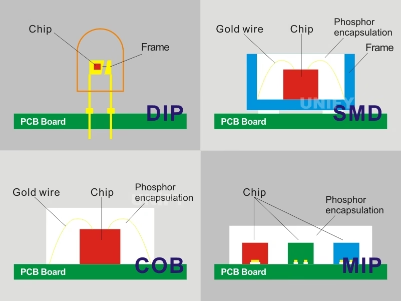
In a wire-bond LED, the chip sits upright on the substrate, and microscopic gold wires connect the chip’s electrodes to the circuit. This is the traditional approach — mature, cost-effective, and still used in most SMD LEDs. However, the gold wires are mechanically fragile, partially block the light-emitting surface, and create longer electrical paths that reduce efficiency.
In a flip-chip LED, the chip is inverted — the light-emitting surface faces upward while the electrodes face downward and bond directly to the substrate. This eliminates gold wires entirely, increases the effective light-emitting area, reduces thermal resistance, and improves luminous efficiency. Flip-chip architecture is the foundation of advanced packaging technologies including COB, MIP, and Micro LED.
What Is DIP LED Display Packaging Technology? The Pioneer Generation (1980s–2000s)
How DIP LED Packaging Works
DIP (Dual In-line Package) was the first commercially viable LED packaging technology. Each DIP LED consists of a single-color LED chip housed inside a plastic or epoxy dome with two long metal leads (pins) that pass through holes drilled in the PCB and are soldered on the opposite side. The dome acts as a lens, focusing the light into a narrow, high-intensity beam.
Why DIP Dominated Early Outdoor Displays
Three characteristics made DIP the default choice for early LED billboards and stadium displays:
- Extreme brightness: DIP LEDs routinely exceed 10,000 nits — far brighter than any SMD equivalent. The lensed dome concentrates light into a directional beam, making content readable even in direct sunlight.
- Rugged durability: The through-hole mounting and robust plastic housing withstand decades of rain, wind, and temperature cycling. Many DIP displays installed in the 1990s are still operational.
- Simple manufacturing: Through-hole soldering is among the most forgiving electronic assembly processes, enabling low-cost production with minimal equipment investment.
DIP Limitations and Modern Niche Applications
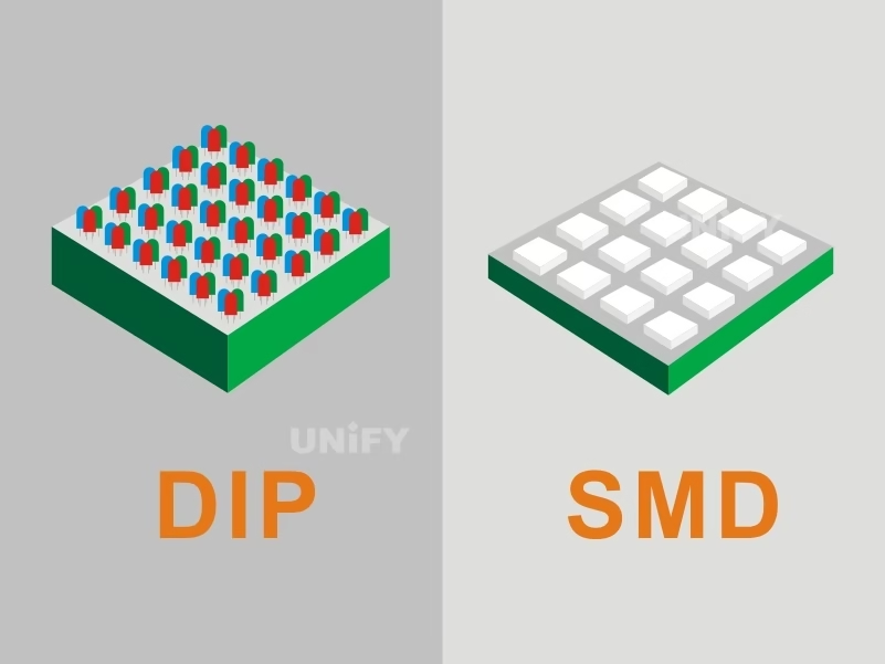
The DIP form factor imposes hard limits: the package is physically large (typically 3–5mm diameter), restricting pixel pitch to P10 at minimum and P16–P20 typically. Resolution is low, power consumption is high, and only single-color chips fit inside each package — a full-color DIP display requires three separate LEDs (R, G, B) per pixel, tripling the component count.
Today, DIP survives in specific outdoor niches where its brightness advantage remains decisive: large-format highway billboards, stadium perimeter displays viewed from 30m+, and permanent outdoor signage where maintenance access is difficult and durability trumps resolution.
How Does SMD LED Display Packaging Technology Work? The Mainstream Standard (2000s–Present)
The Packaging Innovation That Changed Everything
SMD LED packaging integrates red, green, and blue chips into a single compact plastic lamp that is soldered directly onto the PCB surface — no through-holes required. This seemingly simple change had profound consequences for the entire LED display industry. By placing all three RGB chips inside one package, SMD solved the color-mixing problem that plagued DIP displays. It also dramatically reduced the physical footprint per pixel, enabling pixel pitches down to approximately P0.9 before hitting the limits of traditional wire-bond SMD architecture.
SMD Advantages: Why 80% of LED Displays Use This Technology
- Mature, cost-effective manufacturing: SMD assembly uses standard pick-and-place machines operating at 30,000–50,000 components per hour. The global supply chain for SMD LEDs is deep and competitive.
- Wide viewing angles: The flat package design provides 140–160° viewing angles with good color consistency — essential for indoor applications where viewers spread across a room.
- Easy field maintenance: Individual SMD lamps can be replaced on-site with basic tools. This is a significant operational advantage over COB, where module-level replacement is typically required.
- Moderate durability: SMD displays perform well in controlled indoor environments and semi-outdoor installations with proper enclosure design.
Where SMD Reaches Its Limits
SMD packaging begins to show weakness below P1.2: the physical lamp size limits how closely pixels can be placed, wire-bond failures become more common at smaller scales, and the air gap between individual lamps creates visible pixelation at close viewing distances. For fine pitch LED display applications requiring P1.2 or below, advanced packaging technologies become necessary.
Why Is COB LED Display Packaging Technology the Durability Breakthrough? (2010s–Present)
A Fundamentally Different Manufacturing Philosophy
COB represents a radical departure from SMD. Instead of packaging individual LEDs into lamps and then soldering those lamps onto a PCB, COB mounts bare LED chips directly onto the PCB substrate, connects them via microscopic wire bonds (or flip-chip bonding), and then encapsulates the entire surface under a continuous layer of epoxy resin. The result is a single, seamless, solid-state light-emitting surface.
This approach eliminates the LED lamp as a discrete component — and with it, the primary failure modes of SMD displays: lamp detachment from the PCB, physical impact damage to individual LEDs, and moisture ingress between the lamp and the board.
COB Advantages for B2B Applications
- Ultra-fine pixel pitch capability: COB routinely achieves P0.6–P1.2, with some manufacturers reaching P0.4. See our COB LED screen product page for specifications.
- Superior durability: The continuous epoxy layer makes the display waterproof, dustproof, anti-static, and impact-resistant.
- Exceptional contrast: The black epoxy surface absorbs ambient light, producing 10,000:1+ contrast ratios without the reflections that plague SMD surfaces.
- Wider effective viewing angles: The flat, continuous surface maintains color accuracy even at 170° off-axis.
- Lower dead pixel rate: Physical damage during transport and handling — the leading cause of SMD dead pixels — is virtually eliminated.
The COB Repair Challenge
The trade-off B2B buyers must understand: individual pixel repair on COB is not practical in the field. A failed pixel requires replacing the entire module or a designated sub-section using specialized equipment. The counter-argument is that COB modules fail far less frequently than SMD modules — the dead pixel rate can be 10–50× lower. For mission-critical installations, this net reliability gain outweighs the more complex repair procedure.
What Are GOB, IMD, and MIP LED Display Packaging Technologies? The Bridge Solutions
GOB (Glue-on-Board): Enhancing SMD Without Replacing It
GOB is not a new LED packaging technology — it is a protective process applied on top of finished SMD modules. A transparent epoxy glue layer is coated over the entire module surface, encapsulating both the PCB and the SMD lamps beneath a sealed protective layer. The result is an SMD display with significantly improved impact resistance, waterproofing, and dust protection — at roughly half the cost premium of COB.
GOB is particularly popular for rental LED displays and high-traffic indoor environments where the image quality of SMD is sufficient but extra physical protection is needed against frequent handling, setup/teardown cycles, and accidental impact. For a complete comparison, read our guide on SMD vs COB vs GOB.
IMD (Integrated Matrix Device): Multi-Pixel SMD
As pixel pitch demands dropped below P1.0, individual SMD lamps became too small to handle reliably. IMD solves this by integrating 2–4 RGB pixels into a single package — typically a “4-in-1” configuration. This improves structural stability during manufacturing while maintaining the field-repairability advantages of SMD. IMD served as the bridge between traditional SMD and COB for fine-pitch displays in the P0.6–P0.9 range, though it has been largely superseded by COB for new premium installations.
MIP (Mini/Micro LED in Package): The Future Bridge
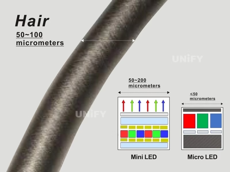
MIP (Mini/Micro LED in Package) represents the latest evolution. Mini or Micro LED chips (under 200 microns) are flip-chip-bonded into individual packages, creating independent, stable light-emitting units that are then mounted onto modules using standard SMT processes. MIP serves as a critical bridge: it enables manufacturers to leverage existing SMT production lines for next-generation chip sizes, avoiding the massive capital investment required for pure COB or Micro LED mass-transfer production.
For B2B buyers, MIP is worth monitoring because it promises to combine the field-repairability of SMD with the pixel density of COB — potentially offering the best of both worlds as manufacturing costs decrease.
When Will Mini LED, Micro LED, and COG LED Display Packaging Go Mainstream?
Mini LED Direct-View: Commercial Reality
Mini LED (chip size 50–200 microns) is not a packaging type per se — it is a chip-size category that is typically implemented using COB or MIP packaging. Mini LED direct-view displays achieve pixel pitches from P0.3 to P1.5, making them the enabling technology for 4K and 8K resolution on standard-sized walls. These displays are commercially available today for high-end broadcast, virtual production (XR stages), and premium corporate environments.
Micro LED: Technical Pinnacle, Commercial Challenge
Micro LED (chip size under 50 microns) represents the theoretical endpoint of LED display evolution: pixel-level self-emission with perfect blacks, 10,000+ nits peak brightness, and 100,000+ hour lifespan. However, the mass transfer process — picking and placing millions of microscopic LEDs with micron-level precision — remains extraordinarily difficult and expensive. Micro LED is commercially viable only for luxury residential and specialized early-adopter projects with effectively unconstrained budgets.
For most B2B buyers in 2026, Mini LED vs alternatives is the relevant comparison — Micro LED remains a technology to watch, not to buy.
COG (Chip-on-Glass): The Glass Substrate Alternative
COG replaces the traditional PCB substrate with glass — an ultra-flat, dimensionally stable material that enables pixel pitches below P0.1. By bonding LED chips directly onto glass, COG opens the door to Micro LED displays with exceptional flatness and uniformity. COG is still primarily in R&D and early commercialization stages, but it represents one of the most promising paths toward affordable Micro LED manufacturing at scale.
LED Display Packaging Technology Comparison: DIP vs SMD vs COB vs MIP
The following table provides a practical comparison of seven LED packaging technologies available to B2B buyers in 2026. Use this to cross-reference supplier specifications against your project’s actual requirements.
| Technology | Era | Min. Pixel Pitch | Durability | Repairability | Relative Cost | Best B2B Application |
|---|---|---|---|---|---|---|
| DIP | 1980s– | P10+ | Very High | Easy (per LED) | $ (lowest) | Highway billboards, stadiums, outdoor signage at 20m+ |
| SMD | 2000s– | P0.9+ | Moderate | Easy (per lamp) | $$ | Indoor commercial, retail, rental, churches, corporate |
| GOB | 2015– | P1.5+ | High | Moderate | $$$ | Rental stages, high-traffic indoor, semi-outdoor |
| IMD | 2018– | P0.6+ | Moderate | Moderate | $$$ | Early fine-pitch indoor, control rooms |
| COB | 2018– | P0.4+ | Very High | Complex (module-level) | $$$$ | Broadcast, command centers, luxury retail, close-viewing |
| MIP | 2023– | P0.3+ | High | Moderate (evolving) | $$$$ | Next-gen fine pitch, Micro LED bridge applications |
| Micro LED | 2025– | P0.1+ | Very High | Very Complex | $$$$$ (highest) | Luxury residential, flagship retail, specialized early-adopter |
How to Choose the Right LED Display Packaging Technology: A B2B Decision Framework
Match Packaging to Environmental Exposure
This is the single most important selection criterion, and the one most commonly overlooked:
- Controlled indoor (conference rooms, retail, lobbies): SMD is the default choice. The cost premium of COB is rarely justified unless viewing distance demands fine pitch below P1.2.
- High-traffic indoor (rental stages, exhibitions, interactive floors): GOB provides the impact and moisture protection these environments demand at a moderate premium over SMD.
- Semi-outdoor / harsh indoor: COB or GOB. The protective encapsulation pays for itself through reduced failure rates.
- Full outdoor (billboards, building façades): DIP for viewing distances above 20m; high-brightness SMD (5,000+ nits) for closer viewing; COB where premium outdoor image quality is required.
Factor Repair Complexity into Total Cost of Ownership
SMD’s field-repairability is genuinely valuable for installations where downtime is costly but on-site technical staff are available. COB’s lower failure rate is more valuable for installations where access is difficult (high mounting, integrated architecture) or downtime is unacceptable (broadcast, control rooms, 24/7 operations). The math is straightforward: multiply your expected module failure rate by the cost of one service visit (labor + travel + downtime) and compare across technologies over a 5-year horizon.
Demand Packaging Documentation from Suppliers
Not all SMD, COB, or MIP is created equal. When evaluating a LED screen manufacturer, request:
- Wire-bond vs flip-chip specification: Flip-chip COB is significantly more reliable than wire-bond COB
- Bin-matching documentation: LED chip wavelength and brightness binning reports for your specific batch
- Encapsulation material datasheet: For COB/GOB, the epoxy formulation determines long-term yellowing and delamination resistance
- Dead pixel warranty terms: Premium manufacturers guarantee far fewer than the industry-standard 1/10,000 dead pixels
For buyers concerned about long-term reliability, our LED screen lifespan guide details the factors that determine how long your investment will perform.
FAQ: LED Display Packaging Technology – Everything B2B Buyers Need to Know
The LED chip is the semiconductor that generates light. The LED package is the complete assembly that includes the chip plus its electrical connections, thermal management structure, optical lens, and protective housing. The package — not the chip alone — determines most of the performance characteristics that matter to B2B buyers, including brightness efficiency, viewing angle, durability, and pixel pitch capability.
COB manufacturing requires higher-precision equipment, has lower throughput (fewer units per hour), and generates higher yield loss during production. Additionally, the epoxy encapsulation process adds material and curing time. However, the total cost of ownership over 5+ years often favors COB for demanding applications because the failure rate is 10–50× lower, reducing service visits and module replacement costs.
Yes — high-brightness SMD displays (5,000–8,000 nits) with proper IP65-rated cabinet enclosures perform well in outdoor environments. However, the SMD lamps themselves are more vulnerable to moisture ingress and UV degradation than DIP or COB alternatives. For permanent outdoor installations, factor in a 3–5 year module replacement cycle for SMD versus 7–10+ years for DIP or COB.
Flip-chip LED architecture inverts the traditional chip orientation — the light-emitting surface faces upward while electrodes bond directly to the substrate below. This eliminates gold wire bonds, which are the #1 failure point in traditional wire-bond LEDs. Flip-chip LEDs have larger effective light-emitting area, lower thermal resistance, and higher luminous efficiency. They are the foundation technology for premium COB, MIP, and Micro LED displays.
MIP and COB are complementary rather than directly competing. COB offers superior surface uniformity, contrast, and protection. MIP offers better compatibility with existing SMT production lines and potentially easier field repair. As of 2026, COB is the more mature and widely deployed technology for fine-pitch commercial applications. MIP is gaining traction and may become the preferred approach as Micro LED chip sizes approach commercialization.
Industry consensus suggests Micro LED will remain an early-adopter technology through at least 2028–2030. The mass transfer manufacturing bottleneck — picking and placing millions of micron-scale LEDs with near-zero defect rates — has not yet been solved at commercial scale. For B2B buyers planning projects in 2026–2028, COB and MIP are the practical premium options. Monitor Micro LED progress but do not budget for it unless your project timeline extends beyond 2028 and your budget is effectively unconstrained.
Why LED Display Packaging Technology Is the Hidden Factor in Every Purchase Decision
The evolution from DIP to SMD to COB to MIP is not merely a technical curiosity — it is the story of how LED displays evolved to serve an ever-widening range of B2B applications, each with distinct requirements for resolution, durability, and total cost of ownership. The packaging technology inside your display determines how long it will last, how it will perform under stress, and how much it will cost to maintain over its service life.
Three principles to guide your next procurement decision:
- SMD remains the rational default for the vast majority of indoor commercial applications. It is mature, cost-effective, field-repairable, and supported by a deep global supply chain.
- COB is worth the premium when failure is expensive. For control rooms, broadcast studios, luxury retail, and any installation where downtime or service access is costly, COB’s superior reliability provides genuine ROI.
- Do not pay for packaging technology your application does not need. A DIP display is the correct choice for a highway billboard viewed from 30 meters. SMD at P1.5 is the correct choice for a corporate lobby viewed from 3 meters. The “best” packaging technology is the one that matches your specific viewing distance, environment, and operational requirements — not the one with the newest acronym.
At UnifyLED, we manufacture displays across the full packaging technology spectrum — DIP, SMD, GOB, and COB — and we help buyers select the right one based on engineering requirements, not sales targets. Contact our team for a packaging technology consultation specific to your project.
Email: legidatechled@gmail.com | WhatsApp: +86-191-18802497