LED Display Basics
- Home
- »
- LED Display Technology
- »
- LED Display Basics
Table of Contents
LED Display Technology and Features
1.LED Display Technology and Composition
LED display technology and its development stages
(1) LED display technology.
An LED display panel is composed of multiple LEDs. It displays various information such as text, graphics, imagdisplay equipment.es, animations, market data, videos, and video signals by turning LEDs on and off. The light color and luminous efficiency of an LED are related to the material and manufacturing process. Currently, red, green, and blue are widely used. Due to the low working voltage of LEDs (1.5-3V), their ability to actively emit light with a certain brightness that can be adjusted by current, their impact resistance, vibration resistance, and long lifespan (100,000 hours), they are widely used in large-scale
An LED display made by placing red and green LEDs together as one pixel is called a dual-color or color screen; one made by placing red, green, and blue LEDs together as one pixel is called a tri-color or full-color screen. The pixel size of indoor LED displays is generally 2-10mm, while for outdoor displays it is mostly 12-26mm. Each pixel consists of several single-color LEDs. The common finished product is called a pixel tube. A dual-color pixel tube is generally composed of 3 red and 2 green LEDs, and a tri-color pixel tube is composed of 2 red, 1 green, and 1 blue LED.
Whether it’s a monochrome, dual-color, or tri-color LED display, to show an image, the brightness of each LED constituting a pixel must be adjustable. The fineness of this adjustment is the grayscale level of the LED display. The higher the grayscale level, the more delicate the displayed image and the richer the colors, and the more complex the corresponding display control system. Generally, for an image with 256 grayscale levels, the color transition is very soft, while for a 16-level grayscale color image, the color transition line is very obvious. Therefore, color LED displays are required to have 256 levels of grayscale. The following are several forms of LEDs used in displays.
LED (or single lamp). Generally composed of a single LED chip, a reflector cup, a metal anode, and a metal cathode, encapsulated in an epoxy resin shell with light-transmitting and light-concentrating capabilities. One or more (of different colors) single lamps can form a basic pixel. Due to its high brightness, it is mostly used for outdoor LED displays.
LED dot matrix module. A light-emitting matrix is formed by several LED chips, encapsulated in a plastic shell with epoxy resin. It is suitable for row and column scanning drivers, making it easy to form high-density LED displays, and is mostly used for indoor LED displays.
Surface-mount LED (or SMD LED). The LED is packaged using surface-mount technology and can be used for indoor full-color LED displays. It allows for single-point maintenance and can effectively overcome the mosaic phenomenon.
LED in the display has a corresponding brightness control circuit. Under computer control, this circuit can adjust the brightness of each LED in the display to show the desired image or text.
LED displays are a new type of display equipment that developed rapidly worldwide in the late 1980s. With features like high reliability, high brightness, long service life, strong environmental adaptability, high cost-performance ratio, low power consumption, impact resistance, and stable performance, they have quickly become the mainstream product in flat-panel displays. China’s LED display industry started in the early 1990s and has developed rapidly. Since the beginning of the 21st century, the LED display industry has faced good market development opportunities. On one hand, demand is constantly expanding, with strong needs for e-government, government transparency, and public information displays. On the other hand, technological progress has provided innovative technical support for market expansion and the creation of new application areas for LED displays.
The biggest feature of LED displays is that their manufacturing is not limited by area, reaching tens or even hundreds of square meters. They can be used in various indoor and outdoor public places to display text, graphics, images, animations, video images, and other information, having a strong advertising rendering power and shocking effect. Their high brightness, full-color capability, convenient and fast error detection, and free adjustment of LED brightness are the development trends of the market.
(2) Development stages of LED displays.
With the rapid development of the electronics industry in the 1960s, display technology developed rapidly. People researched various display technologies such as PDP laser displays, plasma display panels, LCD liquid crystal displays, and LEDs. As semiconductor manufacturing and processing technology gradually matured and improved, LEDs have increasingly dominated solid-state displays. The reason why LEDs have received wide attention and developed rapidly is that they have many advantages. For example: high brightness, low working voltage, low power consumption, easy integration, simple driving, long life, impact resistance, and stable performance, their development prospects are extremely broad. They are currently developing towards higher brightness, higher weather resistance, higher luminous density, luminous uniformity, and full color.
LED displays are a new information display medium that developed rapidly in the late 1980s. They use dot matrix modules or pixel units composed of LEDs to form a display screen. With characteristics such as high reliability, long service life, strong environmental adaptability, high cost-performance ratio, and low usage cost, they have quickly become the mainstream product in flat-panel displays in just over a decade and have been widely used in the field of information display. The development of LED displays has gone through three stages.zz’z
Before 1990 was the growth and formation period of LED displays. On one hand, limited by LED materials and devices, the application fields of LED displays were not widely developed. On the other hand, the control technology of LED displays was basically communication control, which objectively affected the display effect. During this period, LED displays were widely used abroad but rarely in China. The products were mainly red and green dual-primary colors, the control method was communication control, the grayscale level was single-point 4-level gray adjustment, and the product cost was relatively high.
From 1990 to 1995, this stage was a period of rapid development for LED displays. Entering the 1990s, the global information industry grew rapidly, and breakthroughs were constantly made in various fields of information technology. New achievements were also constantly emerging in LED materials and control technology for LED displays. The successful development of blue LED chips brought full-color LED displays to the market. With the technological development in computers and microelectronics, video control technology appeared in the field of LED display control technology. The grayscale level of LED displays reached 16 levels and 64 levels, and the dynamic display effect of LED displays was greatly improved. During this stage, LED displays developed very rapidly in China, from a few enterprises with an annual output value of tens of millions of yuan in the initial stage to dozens of enterprises with an annual output value of several hundred million yuan. The product application fields involved finance and securities, sports, airports, railways, stations, road traffic, commercial advertising, postal services, telecommunications, and many other fields. In particular, the development of the securities and stock industry in 1993 triggered a substantial growth in the LED display market. The mainstream product status of LED displays in the flat-panel display field was basically formed, and the LED display industry became an emerging high-tech industry.
Since 1995, the development of LED displays has entered a period of overall steady improvement and adjustment and perfection of the industrial structure. During this period, competition within the LED display industry intensified, product prices fell sharply, application fields became broader, and a series of new problems appeared in product quality, standardization, etc. Relevant departments paid attention to the development of LED displays and carried out appropriate regulation and guidance. This work is currently being gradually deepened.
(3) Development stages of large-screen LED displays.
First generation: Monochrome LED displays. Based on a single red color, they mainly display text and simple patterns, primarily used for notifications, announcements, and passenger flow guidance systems.
Second generation: Dual-primary color multi-grayscale LED displays. Based on red and yellow-green colors. Since there is no blue, it can only be called pseudo-color. It can display multi-grayscale images and videos. It is currently widely used in telecommunications, banking, taxation, hospitals, government agencies, and other occasions in China, mainly displaying slogans, public service advertisements, and corporate image promotion information.
Third generation: Full-color multi-grayscale LED displays. Based on red, blue, and yellow-green colors, it can display more realistic images and is gradually replacing the previous generation of products.
Fourth generation: True-color multi-grayscale LED displays. Based on red, blue, and pure green colors, it can truly reproduce all the colors of nature (even exceeding the range of natural colors on the color coordinates). It can display various video images and color advertisements. Its brilliant colors, bright high brightness, and delicate contrast have excellent visual shock in the field of advertising.
The true-color 5mm indoor large screen belongs to the fourth-generation product mentioned above. It has high brightness, is not affected by ambient brightness, is thin, occupies a small space, has rich and bright colors, a wide viewing angle, can be used in spacious hall environments, and has no splicing image loss.
LED Display Composition
An LED display screen is composed of several combinable and spliceable display units (unit display panels or unit display cabinets) that form the screen body, plus a set of appropriate controllers (main control board or control system). Therefore, based on various specifications of display panels (or unit cabinets) combined with controllers of different control technologies, many types of LED displays can be formed to meet the needs of different environments and display requirements. A detailed breakdown of an LED display reveals that it consists of the following parts (taking a more complex synchronous video screen as an example).
(1) Screen Body. The indoor screen body is generally composed of an aluminum alloy (angle aluminum or aluminum square tube) as the inner frame, which carries various circuit boards such as the display panel and switching power supply. The outer frame is made of aluminum alloy square tube, or aluminum alloy wrapped in stainless steel, or an integrated sheet metal structure. The frame of an outdoor screen is generally made of angle steel or I-beam depending on the size and load-bearing capacity of the screen body. The outer frame can be decorated with aluminum-plastic panels.
(2) Display Unit. The display unit is the main part of the LED display, consisting of light-emitting materials and driving circuits. Indoor screens are various specifications of unit display panels, and outdoor screens are unit cabinets.
(3) Main Controller. The main controller buffers, performs grayscale transformation, and reorganizes the input RGB digital video signals, and generates various control signals.
(4) Scanning Control Board. The function of the scanning control board is data buffering, generating various scanning signals and duty cycle grayscale control signals.
(5) Switching Power Supply. It converts 220V AC power into various DC powers to supply the various circuits of the LED display.
(6) Transmission Cable (Twisted-pair transmission cable and optical fiber). The display data and various control signals generated by the main controller are transmitted to the screen body through twisted-pair cables (mainly used in single and dual-primary color LED displays). Full-color screens generally use single-mode optical fiber for transmission.
(7) Special Display Card and Multimedia Card (Video Card). In addition to the basic functions of a computer display card, the special display card for LED full-color screens also outputs digital RGB signals and signals such as row, field, and blanking to the main controller. In addition to the above functions, the multimedia card can also convert input analog signals into digital RGB signals (i.e., video capture).
(8) Computer and its peripherals.
(9) Other signal sources and their external devices. Including computers, TVs, DVDs, VCDs, cameras, etc.
LED Display Features
Features of LED Graphic and Text Displays
LED displays have the following features:
(1) High brightness. Rich and vibrant colors. The brightness of outdoor LED displays is greater than 8000 mcd/m², making them the only large-scale display equipment that can be used outdoors all day.
(2) Long lifespan. The lifespan of LEDs is up to 100,000 hours (ten years) or more.
(3) Wide viewing angle. The viewing angle of indoor LED displays can be greater than 160°, and for outdoor displays, it can be greater than 120°.
(4) Modular structure. The screen area of an LED display can be large or small, from less than one square meter to hundreds or thousands of square meters. It is easy to interface with computers, supports a wide range of software, is convenient and flexible to operate, and provides clear and stable images.
(5) Networked LED displays. Using a networked computer, multiple LED displays can be controlled simultaneously to show different content.
(6) Offline operation. LED displays can also work offline. They can display both text and graphic images, with a rich variety of fonts and styles.
Features of LED Video Displays
(1) Clear picture. Based on human visual characteristics and LED display properties, advanced non-linear scanning technology (γ correction) is used to fully reflect all levels of the picture displayed on the LED video screen. Subtle changes can be clearly presented, greatly improving picture quality. This technology is particularly important for LED video displays with fewer pixels. LED video displays based on non-linear differential display technology (i.e., small differences in the low-brightness area, increasing the number of levels, and gradually increasing the difference when moving to the high-brightness area) create a visual effect of “differential consistency,” thus having a better visual effect.
(2) Good compatibility. LED video displays are compatible with the SVGA mode in computers and can be connected to a variety of video devices.
(3) Simultaneous display with computer image. The screen mapping position is adjustable, using professional control software.
(4) High grayscale technology. LED video displays have a high grayscale level and delicate pictures.
(5) Constant current noise reduction technology. The driver chip of the LED video display uses the advanced 5902 system, which is based on constant current noise reduction technology to minimize the impact of power supply and other noise sources on the LED video display.
(6) Brightness adjustment technology. To adapt to different environments and achieve the best display effect, the LED video display is specially designed with a 32-level automatic and manual brightness adjustment device. This ensures that the entire LED video display can achieve the best display effect in various environments.
(7) Strong convection heat dissipation system. When the LED video display is working, the screen body generates a lot of heat. To ensure that the LED video display operates in a stable state, considering all airflow, a strong convection heat dissipation system is adopted to make the system more stable and reliable.
(8) Media networking. With the advent of the information age, system solutions based on media networking use the LED video display as a network terminal to form a standardized interface, which can directly access standard video signals, audio signals, and other network devices, with strong compatibility.
(9) Perfect power distribution system. The power distribution system has a remote control function, with multiple protection functions such as overcurrent, short circuit, and power failure, and can automatically handle various emergency situations. It has a timed automatic screen on/off function, which can achieve unattended operation, and has multi-channel output and delayed power-on functions. The intelligent power supply can realize automatic fan on/off, automatic overheat protection, and automatic recovery without human maintenance.
LED display classification and evaluation parameters
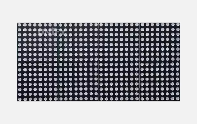
Figure 1-1 φ3.75 LED display
1 LED display classification
(1) Classification by Usage Environment
LED displays are classified by usage environment as follows:
Features: Close viewing distance, high pixel density, small light-emitting points, area typically from less than 1 m² to over ten m².
Environment: Non-direct sunlight or lighting, viewed from a few meters, no sealing or waterproofing.Manufacturing: Light-emitting grains formed into dot matrix modules or numeric tubes, assembled into unit boards, then combined into required sizes.
Specifications: Based on LED single-point diameter: φ3, φ3.75, φ5, φ8, φ10.规格:
Semi-Outdoor LED Display:
Purpose: Information dissemination at doorways, suitable for commercial advertising.
Features: Pixel size between indoor and outdoor, high brightness, usable in non-direct sunlight, partially sealed, often installed under eaves or in windows.
Applications: Bank, mall, or hospital entrances.
Features: Long viewing distance, high brightness (3000–6000 cd/m², varies by orientation), large pixel spacing, low dot density (1000–4000 dots/m²).
Protection: Heat-resistant, windproof, waterproof, lightning-proof.
Manufacturing: Light-emitting grains encapsulated into single LEDs with reflective cups, multiple LEDs form pixel tubes or modules, assembled into sealed unit boxes for waterproofing.
Specifications: Pixel density: 4096, 2500, 2066, 1600, 1024 dots/m²; pixel diameter: φ19, φ22, φ26.
Area: Typically tens to hundreds of m².
(2) Classification by Pixel Spacing
LED displays are classified by pixel spacing as follows:
Named by φ (Indoor Single/Dual-Color):
φ represents light-emitting point diameter (mm).
Specifications: φ3 (60000 pixels/m²), φ3.75 (44000 pixels/m²), φ4.8, φ5 (17000 pixels/m²), φ8.5.
φ3.75 LED display as shown in Figure 1-1
Named by P (Semi-Outdoor Single/Dual-Color, Indoor/Outdoor Full-Color):
P represents distance between light-emitting points (mm).
Outdoor specifications: P10, P12, P16, P20, P25, P30.
Pixel density vs. spacing:
P4: 62500 dots/m²
P4.7: 44300 dots/m²
P6: 27800 dots/m²
P8: 15625 dots/m²
P10: 10000 dots/m²
P11.5: 7500 dots/m²
P12: 6400 dots/m²
P12.5: 6400 dots/m²
P16: 3906 dots/m²
P20: 2500 dots/m²
P25: 1600 dots/m²
P31.25: 1024 dots/m²
P37.5: 711 dots/m²
P40: 625 dots/m²
P45: 495 dots/m²
P50: 400 dots/m²
Size calculation: Spacing × Dot count = Length/Height
Example: PH16 Length=16 dots×1.6 cm=25.6 cm, Height=8 dots×1.6 cm=12.8 cm; PH10 Length=32 dots×1.0 cm=32 cm, Height=16 dots×1.0 cm=16 cm.
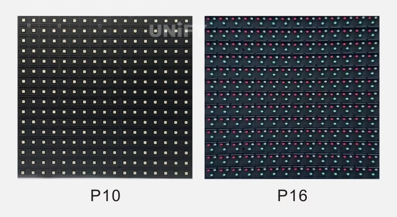
Figure 1-2 P10 and P16 LED displays
(a) P10; (b) P16
Pixel Definition:
Pixel (PIXEL): Smallest independently controllable light-emitting unit.
Tri-color displays: Pixels consist of red, green, blue LED modules, adjustable for any color.
Example: 2 red, 2 green LEDs form 1 pixel.
Pixel with 2 red, 2 green LEDs as shown in Figure 1-3
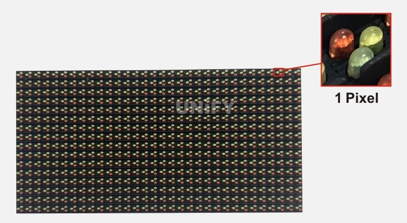
Figure 1-3 A display pixel is composed of 2 red and 2 green pixels.
Pixel Diameter:
Indoor: Single LED, circular, common φ3.0 (60000 pixels/m²), φ3.75 (44000 pixels/m²), φ5.0 (17000 pixels/m²).
Outdoor: Multiple clustered LEDs, non-circular, expressed as average spacing (10, 11.5, 16, 22, 25 mm), pixel density 1024–4096 dots/m².
LED Pixel Modules:
Indoor: 8×8 pixel modules, 8-segment numeric modules.
Outdoor: 4×4, 8×8, 8×16 pixel modules (clustered LED modules).
Pixel Spacing:
Definition: Center-to-center distance between adjacent pixels.
Relationship: Smaller spacing yields higher pixel density, clearer images, larger information capacity, closer viewing distance; larger spacing yields lower density, less information, farther viewing distance.
Examples:
7.62 mm: 17222 pixels/m²
10 mm: 10000 pixels/m²
16 mm: 3906.25 pixels/m²
18.5 mm: 2921.84 pixels/m²
20 mm: 2500 pixels/m²
(3) Classification by Display Color
LED displays are classified by display color as follows:
Single-Color LED Display:
Single color (e.g., red, green, yellow, white, blue).
Each pixel has one color LED, often red (high efficiency), or mixed colors (red, green, yellow LEDs).
Dual-Color LED Display:
Each pixel has red and green LEDs, combining to yellow.
With grayscale control, up to 65535 colors (256 or 512 grayscale levels).
Full-Color LED Display (Tri-Color):
Each pixel has red, green, blue LEDs.
With grayscale control, combines up to 16777216 colors, reproducing natural colors.
(4) Classification by Control Method
LED displays are classified by control method as follows:
Synchronous Control:
Operation: Mimics computer monitors, updates at least 30 frames/s, maps images in real-time, supports multi-grayscale for multimedia advertising.
System: Computer, DVI graphics card, data sending card, synchronous receiving card, HUB board, cables, LED display.
Features: Requires constant connection, displays computer images, 256 grayscale levels (single-color: 256 colors, dual-color: 65536 colors).
Control range example:
φ5: Length 9.76 m, Height 3.9 m
φ3.75: Length 6.1 m, Height 2.448 m
Formula: Control Length = Card dots (length) × Spacing; Control Width = Card dots (width) × Spacing
Asynchronous Control:
Features: Stores and auto-plays data, PC sends data via serial port, offline playback, mainly for text, no multi-grayscale.
System: Unit board, strip card, power supply, optional HUB board.
Advantages: Simple operation, offline capability, one PC controls multiple screens, suitable for networking.
Disadvantages: No animation/image playback, limited storage, small control area (φ5: ≤7 m², φ3.75: ≤2.8 m²).
(5) Classification by Scanning Method
LED displays are classified by scanning method, defined as the ratio of simultaneously lit rows to total rows:
Static Scanning:
Features: All pixels lit simultaneously, common in outdoor full-color displays.
Types: Static real pixel, static virtual.
Advantages: High brightness, high stability.
Disadvantages: High cost, high power consumption.
Dynamic Scanning:
Features: Rows lit sequentially using visual persistence (e.g., 1/2, 1/4, 1/8, 1/16 scans).
Types: Dynamic real pixel, dynamic virtual.
Advantages: Fewer driver chips, energy-efficient.
Disadvantages: Lower brightness, lower stability.
Common Scanning:
Indoor single/dual-color: 1/16 scan.
Indoor full-color: 1/8 scan.
Outdoor single/dual-color: 1/4 scan.
Outdoor full-color: Static scan.
Driver Chips: HC595, MBI5026, TB62726, supporting 1/2, 1/4, 1/8, 1/16 scans.
Example (16×8 Full-Color Module, 2R1G1B):
Total pixels: 16×8×(2+1+1)=512, MBI5026 is 16-bit.
32 MBI5026: Static virtual.
16 MBI5026: 1/2 scan virtual.
8 MBI5026: 1/4 scan virtual.
24 MBI5026: Static real pixel.
12 MBI5026: 1/2 scan real pixel.
6 MBI5026: 1/4 scan real pixel.
Scanning Calculation: LED count ÷ 74HC595 count ÷ 8 = Scan fraction.
Real vs. Virtual Pixels:
Real: Each LED contributes to one pixel, high brightness.
Virtual: Software algorithms allow LEDs to contribute to multiple pixels, higher resolution with fewer LEDs.
(6) Classification by Pixel Unit
LED displays are classified by pixel unit as follows:
LED Numeric Display:
Pixel: 7-segment numeric tube.
Uses: Stock quotes, bank rates, price lists, supports remote input, often paired with strip displays for text.
LED Graphic Display:
Pixel: Dot matrix module, displays text and graphics, no grayscale control.
Advantages: Rich fonts, graphic display, one PC controls multiple screens, offline capability.
LED Video Display:
Pixel: Multiple LEDs, one-to-one mapping with computer monitor, 256 grayscale levels.
Functions: Plays videos, animations, supports multimedia card for video signals, high openness.
(7) Classification by Unit Board LED Structure
LED displays are classified by unit board LED structure as follows:
Dot Matrix Module LED Display:
Features: Evolved from indoor pseudo-color dot matrix, low material cost, simple process, stable quality.
Disadvantages: Poor color consistency, noticeable mosaic, poor display quality.
Figure 1-4 Dot matrix module unit board
Direct-Insertion LED Display:
Features: Adopts outdoor elliptical LEDs, high brightness, wide horizontal viewing angle, better color consistency than dot matrix.
Disadvantages: Poor color mixing, limited viewing angle, horizontal color difference, complex processing, high anti-static requirements, resolution rarely exceeds 10000 dots.
Figure 1-5 Plug-in lamp unit board
SMD LED Display:
Features: Triad or triple-in-one packaging, excellent color and angle consistency, best display metrics.
Disadvantages: High cost, complex processing.
Figure 1-6 SMD unit board
Sub-SMD LED Display:
Features: Improved single-lamp design, near SMD in color and angle consistency, lower cost, resolution up to 17200 dots.
Disadvantages: Complex processing, high anti-static requirements.
(8) Classification by Grayscale Level
LED displays are classified by grayscale level as follows:
16, 32, 64, 128, 256 grayscale levels.
Mainstream: 256 grayscale full-color displays, supporting 256×256×256=16777216 colors.
(9) Classification by Light-Emitting Point Diameter or Spacing
LED displays are classified by light-emitting point diameter or spacing as follows:
Indoor: φ3.0, φ3.75, φ4.8, φ5.0, φ8.0.
Outdoor: φ15, φ19, φ26, P8, P10, P16, P20.
Numeric displays (tube size): 2.0 cm (0.8 in), 2.5 cm (1.0 in), 3.0 cm (1.2 in), 4.6 cm (1.8 in), 5.8 cm (2.3 in), 7.6 cm (3 in).
(10) Classification by Pixel Density
LED displays are classified by pixel density as follows:
2500, 3906, 5102, 6944, 10000, 12384 (3906×4), 15625, 17199, 17772, 27778, 44321, 62500 dots/m².
(11) Classification by Installation Method
LED displays are classified by installation method as follows:
Column (single or dual), wall-mounted, suspended, embedded.
(12) Classification by Purpose
LED displays are classified by purpose as follows:
Information release, traffic guidance, advertising, vehicle-mounted, stadium, stage rental, staircase LED displays.
Traffic Guidance LED Display:
Features: Public-facing, requires high real-time, accuracy, reliability.
Requirements: Stable control systems, software, LED tubes, ICs, high security in network environments.
Design considerations: Location, display type, technical parameters, control system, structure, supporting infrastructure.
(13) Classification by Function
LED displays are classified by function as follows:
Strip Display: Displays text, includes 16×16 or 24×24 dot matrix font library, operates independently, supports remote or computer input, offline capable.
Graphic Display: Displays text and graphics, no grayscale control, rich fonts, offline capable, one PC controls multiple screens.
Video Display: Pixels map one-to-one with computer monitor, 256 grayscale levels, plays videos/animations, high openness.
(14) Classification by Shape
LED displays are classified by shape as follows:
Conventional LED displays, irregular LED displays.
2.Parameters for evaluating LED display screens
(1) Flatness. The surface flatness of LED display screens must be controlled within ±1mm to ensure that the image is not distorted. Local protrusions or depressions will cause blind spots in the viewing angle. The quality of flatness mainly depends on the production process.
(2) Brightness. The brightness of indoor full-color LED display screens should be above 800cd/m², and that of outdoor full-color LED display screens should be above 1500cd/m² to ensure that the image is clearly visible. Brightness is mainly determined by the quality of LED chips.
(3) Viewing angle. The size of the viewing angle directly affects the number of viewers, and the larger the better. It is mainly determined by the packaging method of the LED chip.
(4) White balance effect. This is one of the most important indicators of LED display screens. When the ratio of the three primary colors of red, green, and blue is 1:4.6:0.16, pure white will be displayed. If the actual ratio deviates, white balance deviation will occur. Pay attention to whether the white is blue or yellow-green. The quality of white balance is mainly determined by the control system of the LED display.
(5) Color reproduction. This refers to the color displayed by the LED display being highly consistent with the color of the playback source to ensure the realism of the image. The LED chip has an impact on color reproduction.
(6) Mosaic. This refers to the small square blocks that appear on the LED display that are always bright or always dark, that is, the module necrosis phenomenon. This is mainly due to the poor quality of the connectors used.
(7) Dead point. This refers to a single point that appears on the LED display that is always bright or always dark. The number of dead points is mainly determined by the quality of the LED chip.
(8) Color block. This refers to the obvious color difference between adjacent modules, and the color transition is based on the module. The main reasons for the color block phenomenon are poor control system, low grayscale level, and low scanning frequency.
Factors Determining LED Display Quality and Application Fields
1.Factors Determining LED Display Quality
(1) Brightness and Viewing Angle
An LED display’s brightness is primarily determined by the luminous intensity and density of the LEDs. In recent years, new technologies in substrates, epitaxy, chips, and packaging—especially the stabilization of indium tin oxide (ITO) current spreading layer technology—have significantly increased the luminous intensity of LEDs.
Currently, top-tier small-power LEDs can achieve luminous intensities as high as 4000 mcd for green, 1500 mcd for red, and 1000 mcd for blue, with horizontal viewing angles of 110° and vertical angles of 50°. At a pixel pitch of 20 mm, an LED display’s brightness can exceed 10000 nit, allowing it to work around the clock in any environment.
For a single LED display, the brightness is highest when viewed directly from the front. As you move to the sides, the brightness gradually decreases. The angle at which the brightness drops to half of the frontal brightness is called the viewing angle. A wider viewing angle indicates a better side-viewing effect. LED displays typically have a horizontal and a vertical viewing angle. Generally, indoor screens should have a horizontal viewing angle of over 150°, while outdoor screens should be over 100°.
(2)Uniformity and Clarity
Inconsistent performance parameters among LEDs are the main reason for poor uniformity, which in turn is the primary factor limiting a display’s clarity, not pixel pitch. As LED display technology has evolved, uniformity has become the most important metric for judging quality. Phenomena like the “dust effect” and “mosaic phenomenon” are figurative descriptions of severe non-uniformity between pixels and modules.
The root causes of non-uniformity are:
Inconsistent performance parameters of the LEDs.
Insufficient assembly precision during manufacturing and installation.
Inconsistent electrical parameters of other electronic components, or improper design of modules and PCBs.
The main culprit is “inconsistent LED performance parameters,” which includes variations in luminous intensity, optical axis, color coordinates, light intensity distribution curves for each primary color, and decay characteristics.
There are two primary technical approaches to solve this issue:
Sub-binning: Further subdividing LED specification parameters to improve consistency.
Post-correction: A method to improve uniformity after assembly, which has evolved from early module correction to today’s point-by-point correction. The correction technology has also expanded from simple luminous intensity correction to a combination of luminous intensity and color coordinate correction.
However, post-correction cannot completely eliminate all issues. Inconsistent optical axes, decay characteristics, poor assembly precision, and irregular design cannot be fixed by post-correction; in fact, the correction might even worsen these inconsistencies. Therefore, post-correction is only a “symptom” remedy, while LED parameter sub-binning is the fundamental solution and the future trend for the LED display industry.
It’s a common misconception in the industry to equate resolution with clarity. LED display clarity is a subjective perception that a human eye has of multiple factors, including resolution, uniformity (signal-to-noise ratio), brightness, and contrast. Simply reducing pixel pitch to increase resolution while ignoring uniformity is meaningless for improving clarity. An LED display with a severe “dust effect” or “mosaic phenomenon” cannot produce a clear image, no matter how small its pixel pitch or high its resolution. In this sense, uniformity, not pixel pitch, is the main factor currently limiting the improvement of LED display clarity.
(3)LED Display Pixel Out-of-Control Rate
The pixel out-of-control rate is the proportion of a display’s smallest imaging units (pixels) that are not working correctly. There are two types of pixel failures:
Blind spots: Pixels that should be lit but are not.
Bright spots: Pixels that should be off but remain lit.
An LED pixel is typically composed of 2R1G1B, 1R1G1B, or other combinations of red, green, and blue LEDs. If any single LED within a pixel fails, the entire pixel is considered out of control. For simplicity, the out-of-control rate is calculated for each primary color (red, green, blue) separately, and the maximum value is taken as the display’s overall pixel out-of-control rate.
The ratio of out-of-control pixels to the total number of pixels on the screen is called the whole-screen pixel out-of-control rate. Additionally, to prevent pixel failures from concentrating in one area, the regional pixel out-of-control rate is used. This is the ratio of out-of-control pixels to the total pixels within a 100×100 pixel area (10,000 pixels). This metric provides a quantifiable and intuitive way to enforce the standard that failed pixels should be “discretely distributed.”
Most domestic LED displays are aged before leaving the factory, and any failed pixels are repaired or replaced. The “whole-screen pixel out-of-control rate” is typically controlled to be within 1/104, and the “regional pixel out-of-control rate” is controlled to be within 3/104. Some manufacturers even have a corporate standard of zero failed pixels upon delivery. The acceptable out-of-control rate can vary based on the application. For video playback, a rate of 1/104 is generally acceptable and achievable. For simple character-based information displays, a rate of 12/104 is considered reasonable.
The main cause of pixel failure is LED failure, with electrostatic discharge (ESD) being the biggest trigger. The failure mechanism of LEDs due to ESD is complex, as static electricity can come from equipment, tools, and even the human body. ESD events can range from hundreds to tens of thousands of volts and occur in nanoseconds. The failure of blue and green LEDs during manufacturing, installation, or use is often due to the ESD breakdown of the LED’s PN junction. The International Electrotechnical Commission (IEC) defines three grades of electrostatic discharge sensitivity (ESDS) for devices (human body model): Grade 1 (0-1999V), Grade 2 (2000-3999V), and Grade 3 (>4000V).
Due to the complex production process of LED displays, ESD is difficult to prevent. Therefore, LEDs with an ESDS of Grade 2 or higher are recommended (human body model), and comprehensive static protection measures must be implemented throughout the entire production, installation, and usage process.
(4)Grayscale Levels
Grayscale, also known as gray level or gray scale, refers to the degree of brightness change in a pixel. The grayscale for a single primary color typically ranges from 8 to 1024 levels. For example, if each of the two primary colors has 256 grayscale levels, the display can show 256×256=64K colors, hence it’s called a 256-color display. For digital display technology, grayscale is the key factor determining the number of displayable colors. Generally, a higher grayscale level results in richer colors and a more detailed, delicate image.
Grayscale levels are primarily determined by the system’s A/D conversion bit depth, which requires corresponding support from the video processing chip, memory, and transmission system. Currently, most domestic LED displays use an 8-bit processing system, providing 256 (28) grayscale levels. This allows for 256 brightness variations from black to white. With the RGB primary colors, this creates 256×256×256=16,777,216 colors, commonly referred to as 16 million colors. International brands, however, often use a 10-bit processing system, providing 1024 grayscale levels and enabling over 10.7 billion colors.
While grayscale is crucial for color count, an unlimited increase isn’t always better. The human eye’s resolution is limited, and increasing the system’s bit depth dramatically raises costs for video processing, storage, transmission, and scanning, leading to a decline in cost-effectiveness. Generally, an 8-bit system is sufficient for civil or commercial products, while a 10-bit system is appropriate for broadcast-grade products.
(5) Brightness Discrimination Level
The brightness discrimination level is the number of brightness levels a human eye can distinguish between the darkest and whitest parts of an image. Although a display might have very high grayscale levels (e.g., 256 or 1024), the human eye’s limited sensitivity cannot fully distinguish between all of them. Therefore, many adjacent grayscale levels may appear identical to the viewer. For a display, the more levels the eye can distinguish, the better, as it indicates a larger color space and greater potential for displaying rich colors. This level can be measured with specialized software, and a display that can achieve over 20 levels is considered good.
(6)Grayscale Nonlinear Transformation
Grayscale nonlinear transformation is the process of transforming grayscale data based on empirical or mathematical nonlinear relationships before it is sent to the display. Unlike traditional displays, LEDs have a linear display characteristic. To ensure the LED display’s output is compatible with traditional data sources without losing grayscale levels, a nonlinear transformation is typically performed in the post-processing stage of the LED display system. This transformation increases the bit depth of the data to prevent any loss of grayscale information. The “4096-level” or “16384-level” grayscale claimed by some control system suppliers refers to the grayscale levels after this nonlinear transformation. For example, 4096 levels often use an 8-bit source to a 12-bit space, while 16384 levels use an 8-bit source to a 16-bit space. Like grayscale itself, this parameter is not a “bigger is better” situation; a 12-bit transformation is generally sufficient.
(7)Lifespan
The lifespan of an LED display is determined by various factors. While the lifespan of other components (like power supplies) can be extended through replacement, the LED itself cannot be replaced in large quantities. Therefore, once the LEDs reach the end of their life, the entire display’s lifespan is effectively over. The lifespan of an LED is typically defined as the time it takes for its luminous intensity to decay to 50% of its initial value. Although an LED is often said to have a lifespan of 100,000 hours, this is an assessment under ideal conditions that is not achievable in real-world usage.
A simple experiment and formula can be used to estimate LED lifespan: An LED is run for 1,000 hours under conditions identical to its actual operating environment, and its initial and final luminous intensities are measured. The lifespan can then be calculated using a formula. For example, a well-known brand of blue LED operating at 50°C and 20mA for 1,000 hours might have its final luminous intensity measured at 88% of its initial value. Based on the formula, its lifespan in this environment would be 5,422 hours.
The lifespan of the LED determines the lifespan of the display, but they are not the same. An LED display doesn’t have every LED running at full capacity at all times. When a display is playing normal video content, its lifespan is typically 6 to 10 times that of a single LED. If the LEDs are used at lower currents, their lifespan can be even longer. Therefore, a display using the aforementioned brand of LED might have a lifespan of around 50,000 hours.
LED lifespan can be extended through both device manufacturing and application practices:
Manufacturing: Choosing high-quality epitaxial materials, increasing chip area to reduce current density, balancing current density, reducing thermal resistance, and using high-performance, UV-resistant packaging materials.
Application: Prioritizing heat dissipation in module design, engineering implementation, and maintenance; reducing LED operating currents; and properly configuring LEDs so that the decay rates of all primary colors are synchronized.
(8)Energy Consumption and Efficiency
Improving LED luminous efficiency and reducing the energy consumption of LED displays is a key development direction with several positive implications:
Lower investment in power capacity expansion, power equipment, and cooling systems.
Energy savings, reduced emissions, environmental protection, and lower operating costs.
Reduced display temperature rise, slower LED decay, extended display lifespan, and improved system reliability.
Minimized temperature drift of optoelectronic parameters, leading to more stable image quality.
(9) LED Quality Assurance Technology
Producing high-quality LED displays requires attention to the following aspects:
Anti-static measures: During assembly, proper anti-static measures are essential. These include dedicated anti-static grounding, flooring, soldering irons, mats, wrist straps, clothing, humidity control, and equipment grounding.
Driver circuit layout and wiring design: The layout of driver ICs on the circuit board can affect LED brightness. Poor design with long transmission paths can cause excessive voltage drop, reducing LED brightness.
Current value design: The nominal current for an LED is 20mA, but the maximum operating current should not exceed 80% of this value. For small pixel pitch displays with poor heat dissipation, the current should be even lower.
LED mixing (“混灯”): LEDs of the same color but different brightness must be mixed or arranged according to a designed pattern to ensure consistent brightness across the entire screen.
LED perpendicularity: For through-hole LEDs, manufacturing processes must ensure the LEDs are mounted perpendicular to the PCB. Any deviation can affect the pre-set brightness consistency.
Wave soldering temperature and time control: Wave soldering parameters must be strictly controlled, with a preheat temperature of 100℃±5℃ (not exceeding 120℃) and a soldering temperature of 245℃±5℃ for no more than 3 seconds. After soldering, the LEDs must not be vibrated or impacted until they return to room temperature.
Open solder joint control: More than 50% of the time, an unlit LED is caused by some form of open solder joint. This requires strict process control and enhanced quality inspection, with vibration testing being an effective method before shipping.
Heat dissipation design: LEDs generate heat during operation, and excessive temperatures can negatively impact their decay rate and stability. Therefore, the heat dissipation design of the PCB and cabinet is crucial for extending LED lifespan.
2.Application Fields of LED Displays
LED displays are widely used in a variety of fields:
Securities trading and financial information displays: This sector once accounted for over 50% of the domestic demand for LED displays and remains a major market.
Airport and station dynamic information displays: LED displays are the preferred choice for providing real-time information to travelers.
Port and station passenger guidance systems: LED displays are a key part of automated systems that integrate with broadcasting, arrival/departure systems, and ticketing information.
Stadium information displays: LED displays have replaced traditional incandescent and CRT screens as the main method for displaying information in major sports venues.
Road traffic information displays: Used as variable message signs and speed limit signs in urban traffic and on highways.
Dispatch and command centers: High-density LED displays are increasingly being adopted for power dispatch, vehicle tracking, and fleet management.
Business promotion and information display in service sectors: Used in post offices, telecommunications, and shopping malls for advertising and information dissemination.
Advertising media: In addition to large indoor and outdoor LED billboards, clustered LED display advertising systems are becoming more common in major cities.
Performances and public gatherings: Large LED displays are widely used for live video broadcasts for public and political events, enhancing their impact.
Exhibitions and rentals: Large LED displays are a crucial service provided by exhibition organizers to exhibitors. Professional rental companies also specialize in this service.
Schools and hospitals: Used in schools for announcements and educational content, and in hospitals for publicizing information about medicines and health knowledge.
Common Electronic Components for LED Displays
1LED Devices, Modules, and Unit Boards
LED Devices
The color and efficiency of LEDs are related to the materials and manufacturing processes used. Currently, red, green, and blue (R, G, B) LEDs are widely used. Because LEDs operate at a low voltage (only 1.5V to 3V), can actively emit light with a certain brightness, and are also shock-resistant, vibration-resistant, and have a long lifespan, LED displays remain the primary choice for large-scale display devices.
Two-color screens: A pixel consists of a red and green LED.
Three-color screens (full-color screens): A pixel consists of a red, green, and blue LED.
The pixel size of indoor LED displays is generally 2 to 10 mm, while that of outdoor LED displays is mostly 12 to 26 mm.
Each pixel is composed of several single-color LEDs and is often called a pixel tube. For example, a two-color pixel tube typically consists of three red and two green pixels; a three-color pixel tube consists of two red, one green, and one blue.
The grayscale level of an LED display determines the image’s resolution. The higher the grayscale level, the finer the image and the richer the colors.
An image with 256 grayscale levels has smooth color transitions.
An image with 16 grayscale levels has sharp color transitions.
Therefore, color LED displays are required to achieve 256 grayscale levels.
The main materials that determine LED quality are: the chip, the bracket, the glue (epoxy resin), and the gold wire. The packaging process is also crucial. LEDs for LED displays come in the following forms:
LED lamps (single lamps): High brightness, mostly used for outdoor displays.
LED dot matrix modules: Suitable for row and column scanning, easy to create high-density displays, mostly used for indoor displays.
Surface-mounted LED lamps (SMD LEDs): Used for indoor full-color displays, they allow for single-point maintenance.
LED Die Technical Parameters
Die size: This affects chip heat generation and lifespan. Full-color displays typically use chips larger than 13 mils.
Die brightness: This directly affects display brightness; select a die with a brightness higher than required.
Die wavelength: This directly affects displayed color. Full-color displays typically use positive wavelengths, such as 640nm for red, 525nm for green, and 470nm for blue.
Die uniformity: This affects display uniformity, including brightness and wavelength uniformity.
LED Display Module
Plug-in module: This module uses a DIP package, with the leads soldered through the PCB.
Advantages: Wide viewing angle, high brightness, and good heat dissipation.
Disadvantages: Low pixel density.
Surface mount module: This module uses an SMT package and is soldered directly to the PCB surface.
Advantages: Wide viewing angle, soft image quality, and high pixel density, making it suitable for indoor displays.
Disadvantages: Low brightness and poor heat dissipation.
Sub-surface-mount modules: Between DIP and SMT.
Advantages: High brightness and excellent display quality.
Disadvantages: Complex manufacturing process and difficult maintenance.
The Difference Between 3-in-1 and 3-in-1 Surface-mount Modules
3-in-1 Surface-mount modules: Red, green, and blue chips are packaged in the same package.
Advantages: Simple production and excellent display quality.
Disadvantages: Difficulty in light separation and color separation, high cost.
3-in-1 Surface-mount modules: Red, green, and blue light sources are packaged separately.
Advantages: Low power consumption, good heat dissipation, long life, low maintenance cost, excellent color uniformity, wide viewing angle, and low cost.
3-in-1 Surface-mount modules, with their high cost-performance ratio, are gradually replacing 3-in-1 and sub-surface-mount modules and becoming the mainstream in the market.
Unit Boards/Modules
Indoor unit boards: For example, a 64×32 dot matrix unit board (please insert Figure 1-7 here)
Figure 1-7 Indoor unit board
Semi-Outdoor Module: For example, a 64×32 dot matrix semi-outdoor single-color (red) module
Figure 1-8 Semi-outdoor module
Full-Outdoor Module: Available in various specifications, such as a 32×16 dot matrix single-color (red) module (please insert Figure 1-9(a) here), a 16×8 dot matrix single-color (2R) module (please insert Figure 1-9(b) here), and a 16×6 dot matrix two-color module
Figure 1-9: Full Outdoor Module
(a) 32×16 dot matrix, single color (red); (b) 16×8 dot matrix, single color (2R); (c) 16×6 dot matrix, dual color
3.LED Display Dedicated Chip: Performance Parameters & Comparison
(1)LED Display Dedicated Chip Performance Parameters
An LED display is a large-format flat panel display assembled from display units composed of LEDs and their driver chips. The performance of these chips is crucial for the display quality of the LED screen. In recent years, with the development of the LED market, manufacturers such as Japan’s TOSHIBA and SONY, USA’s Texas Instruments (TI), and Taiwan’s Macroblock (MBI) and Silicon Touch (SITI) have begun to produce dedicated driver chips for LEDs. LED driver chips can be categorized as general-purpose or dedicated.
General-purpose chips are not specifically designed to drive LEDs; they are logic chips with some of the logic functions required for LED displays (such as serial-to-parallel shift registers). General-purpose chips are typically used in low-end LED displays, such as indoor monochrome and dual-color screens. The most commonly used general-purpose chip is the 74HC595. The 74HC595 features an 8-bit latch, a serial-to-parallel shift register, and three-state outputs. Each channel can output a maximum current of 35mA (non-constant current). Most IC manufacturers can produce this type of chip. In the LED display industry, products from manufacturers like Motorola (Onsemi), Philips, and ST are commonly used, with Motorola’s products having better performance.
Dedicated chips are driver chips specifically designed according to the luminous characteristics of LEDs. LEDs are current-characteristic devices, meaning that under saturation, their brightness changes with the current, not by adjusting the voltage across them. Therefore, a primary feature of dedicated chips is providing a constant current source. A constant current source ensures stable driving of the LED, eliminates flicker, and is a prerequisite for high-quality images on an LED display. Some dedicated chips also include special functions to meet the requirements of different industries, such as brightness adjustment and error detection. Dedicated chips feature high output current and constant current, making them suitable for applications requiring large currents and high image quality, such as outdoor full-color and indoor full-color LED displays. Key performance parameters for dedicated chips include maximum output current, number of constant current source outputs, current output error (bit-to-bit, chip-to-chip), and data shift clock.
- Maximum Output Current
The maximum output current of mainstream constant current source chips is mostly defined as the maximum single-channel output current, which is generally around 90mA. Constant current is the most fundamental characteristic of dedicated chips and the basis for achieving high image quality in LED displays. However, the maximum value of constant current that each channel can output simultaneously (i.e., the maximum constant output current) is more meaningful for LED displays, as a white balance state requires every channel to output constant current simultaneously. Generally, the maximum constant output current is less than the allowed maximum output current.
- Number of Constant Current Source Outputs
The number of constant current source outputs mainly comes in two specifications: 8 (8-bit source) and 16 (16-bit source). Currently, 16-bit source chips are mainstream, such as the TLC5921, TB62706/TB62726, and MB15026/MB15016. The main advantage of 16-bit source chips is their reduced size, which facilitates the layout of the LED driver board (PCB), especially for PCBs with a small dot pitch.
- Current Output Error
Current output error is divided into two types: bit-to-bit current error, which is the error between each output channel on the same chip; and chip-to-chip current error, which is the error in output current between different chips. Current output error is a critical parameter that greatly affects the uniformity of the LED display. The larger the error, the worse the uniformity of the LED display, making it difficult for the screen to achieve white balance. Currently, the bit-to-bit current error of mainstream constant current source chips is generally less than ±6%, and the chip-to-chip current error is less than ±15%.
- Data Shift Clock
The basic functions of dedicated LED driver chips include a serial shift register function to facilitate the cascading and transmission of display data for constructing large-scale, multi-pixel LED displays. The data shift clock determines the transmission speed of display data and plays a crucial role in the update rate of the LED display. As a large-scale display device, the refresh rate should be above 85Hz to ensure a stable picture (without a sense of scanning flicker). A high data shift clock is the foundation for an LED display to achieve a high-refresh-rate picture. The shift clock frequency of mainstream constant current source chips is generally above 15MHz.
(2)Performance Comparison of Dedicated LED Chips
The main manufacturers of dedicated LED driver chips include TOSHIBA, TI (Texas Instruments), SONY, MBI (Macroblock Inc.), and SITI (Silicon Touch Technology Inc.). The chips from these companies are all used in the domestic LED display industry.
TOSHIBA
Its products offer a relatively high price-performance ratio. Main products include TB62705, TB62706, TB62725, TB62726, TB62718, TB62719, and TB62727. Among them, TB62705 and TB62725 are 8-bit source chips, while TB62706 and TB62726 are 16-bit source chips. TB62725 and TB62726 are the upgraded versions of TB62705 and TB62706, respectively. These products show improvements in current output error (both bit-to-bit and chip-to-chip), data shift clock, supply voltage, and chip power consumption. As mid-range chips, TB62725 and TB62726 have gradually replaced TB62705 and TB62706. Additionally, the TB62726 has a narrow-body package version, the TB62726AFNA, with a width of only 6.3mm (the surface-mount package width of TB62706 is 8.2mm). This narrow package is suitable for LED displays with a small dot pitch.
Please note: The pin definition of the AFNA package is different from the standard package (rotated 90° counterclockwise).
The TB62718 and TB62719 are driver chips launched by TOSHIBA for the high-end market. In addition to the functions of a standard constant current source chip, they add features like a 256-level grayscale generation mechanism (8-bit PWM), internal current adjustment, thermal shutdown (TSD), and load open detection (LOD). These chips are suitable for high-end full-color LED displays. The TB62727 is a new product from TOSHIBA, primarily adding current adjustment, temperature alarm, and output open detection functions to the TB62726. It is positioned in the market between the TB62719(718) and the TB62726.
TI (Texas Instruments)
Its products are cost-effective. Main products include the TLC5921, TLC5930, and TLC5911. The TLC5921 is a high-precision 16-bit source driver chip with TSD and LOD functions, and its bit-to-bit current error is only ±4%. The TLC5930 is a 12-bit source chip with 1024-level grayscale (10-bit PWM) and a 64-level brightness adjustment function. The TLC5911 is a driver chip positioned for the high-end market, a 16-bit source chip with 1024-level grayscale, 64-level brightness adjustment, TSD, and LOD functions.
Note: There is a metal heat sink under the TLC5921 and TLC5930 chips; in practical applications, care must be taken to avoid contact with the LED pins, otherwise, leakage can cause the LEDs to dim.
SONY
Its products have always been positioned in the high-end market. Main products include the CXA3281N and CXR3596R. The CXA3281N is an 8-bit source chip with a 4096-level grayscale mechanism (12-bit PWM), 256-level brightness adjustment, 1024-level output current adjustment, TSD, LOD, and LSD (load short detection) functions. The CXA3281N is primarily designed for static driving methods, with a maximum output current of 40mA. The CXR3596R is a 16-bit source chip that inherits all the features of the CXA3281N, mainly increasing the output current (from 40mA to 80mA) and the number of constant current source outputs (from 8 to 16).
MBI (Macroblock Inc.)
Its products basically correspond to TOSHIBA‘s mid-range products, and their pins and functions are also fully compatible. Except for a slight difference in the resistance value of the external constant current setting resistor, they can be directly interchanged. MBI‘s MB15001 and MB15016 correspond to TB62705 and TB62706, respectively; MB15168 corresponds to TB62726 (the original text likely meant MB15026, but is preserved for fidelity). Additionally, there are new products with LOD function: MB15169 (8-bit source), MB15027 (16-bit source), and products with 64-level brightness adjustment: MB15170 (8-bit source) and MB15028 (16-bit source). Chips with LOD and brightness adjustment functions use MBI’s Share-I-O™ technology, and their pinouts are fully compatible with chips without these functions, such as the MB15168 and MB15026. This allows for an upgrade to new functions without changing the driver board design.
SITI (Silicon Touch Technology Inc.)
A company specializing in the R&D and production of LED driver chips, its products have stable performance. Its main products include ST2221A, ST2221C, DM134, DM135, DM136, DM133, and ST2226A. Except for the ST2221A, which is an 8-bit source, the rest are 16-bit source chips. The DM134, DM135, and DM136 are upgraded products of the ST2221C. The only difference between these three chips is the output current: DM134 has an output current of 40-90mA, DM135 has an output current of 10-50mA, and DM136 has an output current of 3-15mA. The DM133 has 64-level brightness adjustment, LOD, and TSD functions. The ST2226A has a 1024-level grayscale mechanism (10-bit PWM) and is considered a high-end chip.
Based on the product structures of the major LED driver chip manufacturers mentioned above, current LED constant current chips can be primarily divided into three tiers.
First Tier are chips with a grayscale mechanism. These chips have an internal PWM function that can generate grayscale based on the input data, making it easier to achieve deep grayscale levels and high-quality images.
Second Tier are chips with LOD, TSD, and brightness adjustment functions. These chips, with their additional functions, are more suitable for specific applications, such as variable message signs, as they can detect LED errors.
Third Tier are constant current source chips without any additional functions. These chips only provide a high-precision constant current source for the LEDs, ensuring good quality for the display screen’s picture.
3.Commonly used integrated circuits for LED displays
(1)74HC245
The 74HC245 is an 8-bit bidirectional shift register used in P10 modules for signal power amplification and shaping. The pin arrangement is shown in Figure 1-10. The pin functions are as follows:
- Pin 1 DIR: Used for input/output port switching. When DIR=“1” (high level), signals are input from the A side and output from the B side; when DIR=“0” (low level), signals are input from the B side and output from the A side. In P10 monochrome modules, this pin is connected to high level, meaning signals are always input from A and output from B.
- Pins 2–9: A signal input/output pins. A0=B0, …, A8=B8. A1 and B1 form a pair. If DIR=“1” and G=“0”, A1 is input and B1 is output; if DIR=“0” and G=“0”, B1 is input and A1 is output. Other pairs function similarly.
- Pins 11–18: B signal input/output pins, with the same function as the A side.
- Pin 19 OE: Enable pin, active low. If “1”, A/B signals are not conducted; if “0”, A/B are enabled, acting as a switch. In P10 monochrome modules, this pin is connected to low level, keeping signals always conducted.
- Pin 10 GND: Power ground.
- Pin 20 Vcc: Power positive.
74HC245 Truth Table (see Table 1-1):
| Control Inputs | Operation | Notes |
|---|---|---|
| G | DIR | |
| L | L | B data to A bus |
| L | H | A data to B bus |
Note: H=High level, L=Low level.
Absolute Maximum Ratings:
- Supply voltage (Ucc): -0.5 to 7.0V.
- DC input voltage (between DIR and GND): -1.5 to Ucc+1.5V.
- DC input/output voltage: -0.5 to Ucc+0.5V.
- Clamp diode current (IcD): ±20mA.
- DC output current (per pin): ±35mA.
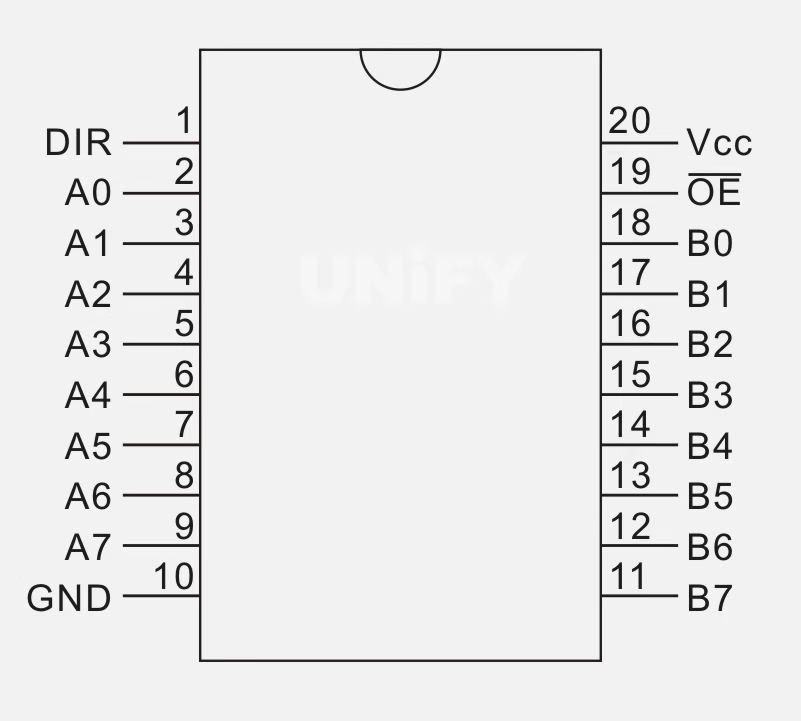
Figure 1-10 74HC245 pinout
(2)74HC04
The 74HC04 is a 6-bit inverter, where the input and output levels are opposite (high input yields low output). A is the input, and Y is the output. The pin arrangement is shown in Figure 1-11. The pin functions are as follows:
- Pins 1–2, 3–4, 5–6, 8–9, 10–11, 12–13: Each pair is independent. In P10 modules, only the OE signal is inverted.
- Pin 7 GND: Power ground.
- Pin 14 Vcc: Power positive.
- Signal input/output: Signals input from A, output inverted from Y. A0 and Y0 form a pair, e.g., A1=“1” results in Y1=“0”, A1=“0” results in Y1=“1”. Other pairs function similarly.
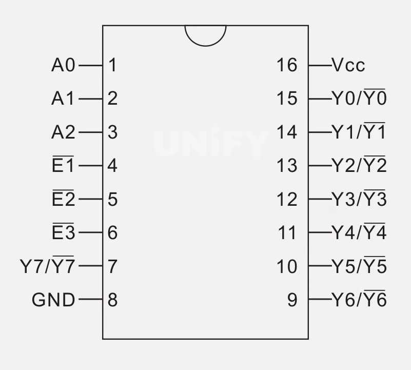
Figure 1-11 74HC04 pinout
(3) 74HC138
The 74HC138 is an 8-bit binary-to-decimal decoder used to select display rows. One 74HC138 can select 8 rows, and P10 modules typically use two 74HC138 chips to select one of 16 rows. The pin arrangement is shown in Figure 1-12. The pin functions are as follows:
- Pins 1–3 A0, A1, A2: Binary input pins. In P10 modules, only A0 and A1 are used; A2 is grounded.
- Pins 4–6: Chip select signal control. Selected only when pins 4 and 5 are “0” and pin 6 is “1”, with output controlled by A0, A1, A2. Other combinations result in no selection, with Y1/Y1–Y7/Y7 outputs all “1”. In P10 modules, pin 4 is grounded, pin 5 connects to pin 2 of 74HC04, and pin 6 connects to power positive, making selection always valid, with output controlled only by the OE signal.
- Pins 7, 9–15: Output pins. Without selection, Y1/Y1–Y7/Y7 outputs are all “1”.
- Pin 8 GND: Power ground.
- Pin 15 Vcc: Power positive.
The 74HC138 accepts 3-bit binary weighted address inputs (A0, A1, A2) and, when enabled, provides 8 mutually exclusive low-active outputs (Y1/Y1–Y7/Y7). It has three enable inputs: E1, E2 (low-active), and E3 (high-active). Unless E1 and E2 are low and E3 is high, all outputs remain high. With composite enable features, four 74HC138 chips and one inverter can form a 1-to-32 (5-line to 32-line) decoder. It can also act as an 8-output demultiplexer.
Technical Parameters:
- Voltage: 2.0–6.0V.
- Drive current: ±5.2mA.
- Propagation delay: 12ns/5V.
- Logic level: CMOS.
- Package types: SO16, SSOP16, DIP16, TSSOP16.
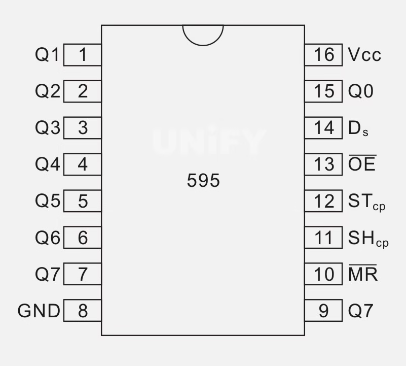
(4)74HC595
The 74HC595 is an 8-bit shift latch with an 8-bit serial-in, parallel-out shift register and an 8-bit output latch, used to drive display columns. Each chip drives 8 columns, and multiple chips can be cascaded. The pin arrangement is shown in Figure 1-13. The pin functions are as follows:
- Pins 1–7 Q1–Q7: Parallel data output.
- Pin 15 Q0: Parallel data output.
- Pin 8 GND: Power ground.
- Pin 9 Q7′: Serial data output.
- Pin 10 MR: Reset pin; resets register data when triggered. In LED displays, typically connected to Vcc.
- Pin 11 SHc: Clock pin; each clock signal shifts one bit into the register.
- Pin 12 STcp: Latch pin; data in the register requires a latch signal to output to Q0–Q7.
- Pin 13 OE: Enable pin; when “1”, Q0–Q7 are all “1”; when “0”, outputs are controlled by input data.
- Pin 14 Ds: Serial data input; display data enters here with clock signal cooperation.
The 74HC595 is a silicon CMOS device, compatible with low-voltage TTL circuits and JEDEC standards. Data is input to the shift register on the rising edge of SHcp and to the storage register on the rising edge of STcp. The shift register has a serial input (Ds), serial output (Q7′), and asynchronous low-level reset. The storage register has an 8-bit tri-state bus output.
Technical Features:
- 8-bit serial input/8-bit serial or parallel output storage register, tri-state output.
- Output register can be cleared directly, 100MHz shift frequency.
- Parallel output, bus driver; serial output.

Figure 1-13 74HC595 pinout
(5)LT4953
The LT4953 is a row driver; each chip can drive 2 display rows. The pin arrangement is shown in Figure 1-14. The pin functions are as follows:
- Pins 1, 3: Connected to Vcc.
- Pins 2, 4: Control pins; pin 2 controls outputs of pins 7 and 8, pin 4 controls outputs of pins 5 and 6. Outputs occur only when pin 2 is “0” for pins 7 and 8, or pin 4 is “0” for pins 5 and 6; otherwise, outputs are high-impedance.
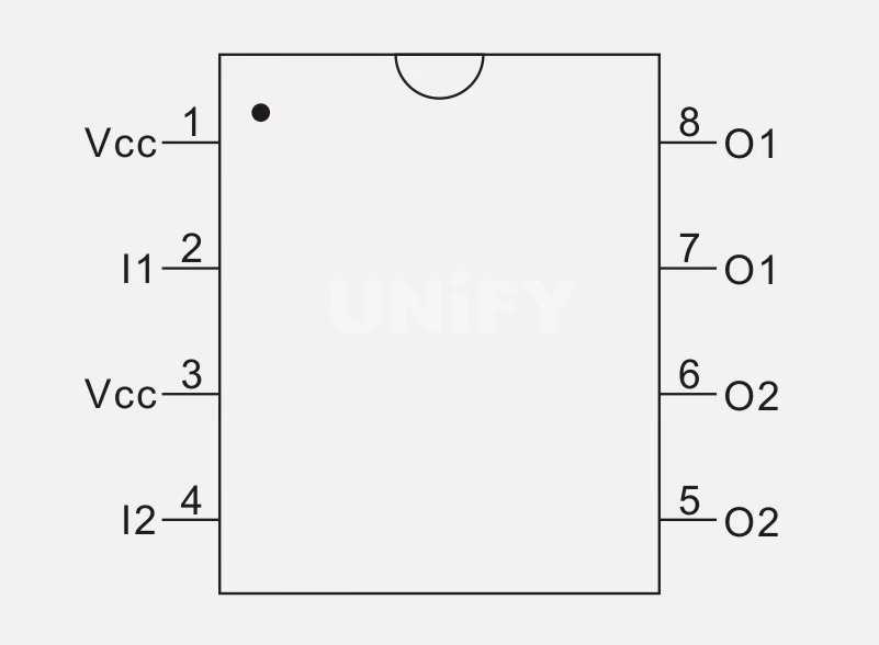
Figure 1-14 LT4953 pinout
(6)MBI5026
The MBI5026 is a 16-bit shift latch, with pin arrangement shown in Figure 1-15. The pin functions are as follows:
- Pin 1 GND: Power ground.
- Pin 24 VDD: Power positive.
- Pin 2 SDI: Serial data input.
- Pin 3 CLK: Clock signal input.
- Pin 4 LE: Latch signal input.
- Pin 23 R-EXT: Output current adjustment, connected to a resistor.
- Pin 22 SDO: Serial data output.
- Pin 21 OE: Enable input.
- Pins 5–20 OUT0–OUT15: Current output pins.
MBI5026 functions similarly to 74HC595 but is a 16-bit shift latch with output current adjustment. Outputs have no high level, only high-impedance and low-level states. It is interchangeable with TB62726.
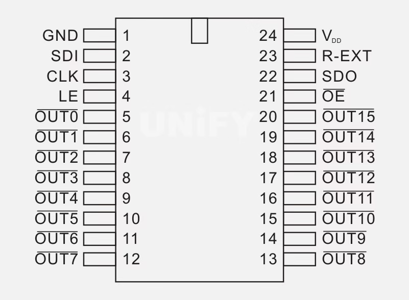
Figure 1-15 MBI5026 pinout
(7)TB62726
The TB62726 is a 16-bit shift latch, sometimes used instead of 74HC595 to drive 16 columns. The pin arrangement is shown in Figure 1-16. The pin functions are as follows:
- Pin 1 GND: Power ground.
- Pin 24 VDD: Power positive.
- Pin 2 SERIAL-IN: Serial data input.
- Pin 3 CLOCK: Clock input.
- Pin 4 LATCH: Latch input.
- Pin 23 R-EXT: Output current adjustment, connected to a resistor.
- Pin 22 SERIAL-OUT: Serial data output.
- Pin 21 ENABLE: Enable input.
- Pins 5–20 OUT0–OUT15: Current output pins.
TB62726 functions similarly to 74HC595 but is a 16-bit shift latch with output current adjustment. Outputs have no high level, only high-impedance and low-level states. It is interchangeable with MBI5026.
Technical Characteristics:
- Output current capacity and channels: 90mA×16.
- Constant current range: 2–80mA.
- Output voltage: 0.7V (output current 2–80mA); 0.4V (output current 2–40mA).
- Operating voltage range: 3.0–5.5V.
- Suitable for common-anode LEDs.
- Input signal voltage: 3.3V CMOS voltage.
- Maximum output terminal voltage: 17V.
- Continuous transfer rate: 20MHz (cascade limit).
- Operating temperature range: -40 to 85℃.
- Package types: SDIP24-P-300-1.78, SSOP24-P-300-1.00B.
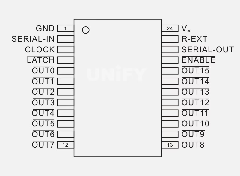
Figure 1-16 TB62726 pinout
(8)SMT5026
The SMT5026 is a 16-channel constant-current LED driver IC designed for LED displays, with built-in CMOS shift register and latch functions, converting serial input data to parallel output data. It provides 16 constant-current outputs (5–90mA, adjusted by external resistor). It uses advanced BiCMOS technology for high-precision constant-current output. The pin arrangement is shown in Figure 1-17.
Product Characteristics:
- 16 constant-current source output channels, unaffected by load voltage changes.
- Constant-current output range: 5–90mA.
- Precise current matching: maximum channel error <±1.5%, maximum chip error <±3.0%.
- Constant-current output adjustable via external resistor (Iout=5–90mA).
- Data transfer clock frequency up to 25MHz, with Schmitt trigger input for enhanced noise immunity.
- Fast output current response, OE (minimum) ≤200ns.
- Operating voltage: 3.0–5.5V.
- RoHS compliant, 100% lead-free packaging.
- Package types: SSOP24-300-1.0, SSOP24-150-0.635, compatible with mainstream products (Pin to Pin).
Figure 1-17 SMT5026 pinout
4.LED Display Driver Chip Comparison
(1) TLC5941 Driver Chip
TLC5941, developed by Texas Instruments (TI), is a high-performance LED display driver chip with the following features:
Functionality: Supports dot correction and high grayscale levels (PWM control), with all internal data registers, grayscale registers, dot correction registers, and error status information accessed via a serial interface.
Electrical Characteristics:
Maximum serial clock frequency: 30 MHz.
Chip-to-chip current error: Within ±6%.
Bit-to-bit current error: Within ±4%.
Maximum output current per channel: 80 mA.
Grayscale Control:
Each channel supports 12-bit PWM control, providing 4096 grayscale levels.
6-bit dot correction registers offer 64-level current control, with maximum current set via external resistors.
64-level current control enables LED dot grayscale correction, and 4096 grayscale levels ensure up to 256 levels even at low grayscale.
Full-color LED displays achieve 16M colors (256×256×256).
Design Advantages:
PWM grayscale control is independent of serial data output, reducing design complexity and enabling high frame rates for excellent dynamic display effects.
Centralized PWM control simplifies tasks for programmable logic chips or high-speed CPUs, focusing only on buffer management and data output.
Reliability Features:
Provides LED open detection (LOD) and thermal shutdown (TSD).
Built-in open-collector output circuit pulls the output pin low on error, enabling system self-diagnosis via pull-up resistors and high-level signal monitoring.
Applications: Harsh environments, high display quality, and high safety requirements, such as highway LED information signs and large outdoor LED TVs.
(2) MBI5028 Driver Chip
MBI5028, developed by Macroblock, is an LED display driver chip with programmable current gain, featuring:
Functionality:
Includes serial-to-parallel shift registers and output latches, using PrecisionDrive technology for enhanced electrical characteristics.
Maximum serial clock frequency: 25 MHz.
Chip-to-chip current error: Within ±6%.
Bit-to-bit current error: Within ±3%.
Maximum output current: 90 mA.
Current Gain Control:
Uses Share-IO technology, requiring no additional pins; enters current adjustment mode via specific signal sequences.
System microcontroller writes data to the current gain control logic, latched and controlled via a digital-to-analog shared converter.
Brightness Compensation:
Programmable current gain and PrecisionDrive technology adjust current deviations, compensating for brightness reduction due to environmental changes or LED aging.
Provides 256 current levels, achieving a 1200% dynamic range for improved imaging quality.
Compatibility:
Compatible with MBI5026, allowing upgrades without PCB redesign, reducing costs.
Applications: Environments with moderate conditions but requiring high-quality imaging, such as indoor large LED displays for mid-to-low-end applications.
(3) ST2221C Driver Chip
ST2221C, developed by Sitronix Technology, is an LED display driver chip for low-end applications, with the following features:
Functionality:
Includes serial-to-parallel shift register, output latch, and current output control units.
Contains 16 constant-current driver channels, capable of driving 16 LEDs simultaneously.
Electrical Characteristics:
Maximum serial clock frequency: 25 MHz.
Chip-to-chip current error: Within ±10%.
Bit-to-bit current error: Within ±6%.
Maximum output current: 120 mA.
Applications: Low-end LED displays, such as indoor information screens.
Table 1-2 Comparison of Three LED Display Driver Solutions
Model | Max Current/mA | Bit-to-Bit Error | Chip-to-Chip Error | Clock Frequency/MHz | Advantages | Disadvantages |
|---|---|---|---|---|---|---|
TLC5941 | 80 | ±4% | ±6% | 30 | High speed, low current error, LOD/TSD functions, wide application range | Low max current, expensive, high engineering cost, poor compatibility |
MBI5028 | 90 | ±3% | ±6% | 25 | High speed, higher max current, low current error, good compatibility | Fewer functions, limited application range |
ST2221C | 120 | ±6% | ±10% | 25 | High speed, high max current, low cost, good compatibility | Fewer functions, limited application range, high current error |
Comparison of three LED display driver solutions as shown in Table 1-2, please insert table here * *
(4) LED Display Driver Chip Issues
LED display driver chips face the following challenges:
Power Consumption and Heat Dissipation:
Issue: High output current leads to significant power consumption and heat, a primary barrier to driver chip development.
Impact: Particularly critical for future handheld LED display applications.
Solution: Advances in LED manufacturing and reduced drive currents will gradually mitigate this issue.
Application Cost:
Current State: A mainstream 16-bit constant-current driver chip supports only 16 LED channels, requiring multiple chips for a 1024×768 display, increasing material costs.
Improvement: Scanning-based driver chips can drive multiple LEDs at once, significantly reducing application costs.
LED display data interface and scanning method
1. LED Display Data Interfaces
To input display signals into modules, modules often use a 2×8 pin header. A 16PIN flat cable (FC) connector is used to connect modules to the LED display control card and to other modules. The arrangement of the signals on each pin is called an interface. Common interfaces include 08, 12, and 04, as shown in Figure 1-18. The LED display interface is used to connect the control card to the unit board/module to transmit control signals. Different scanning methods require different interfaces, but the principle is the same; the main difference is the arrangement of the signal lines. If the unit board interface is inconsistent with the control card, a conversion cable needs to be made.
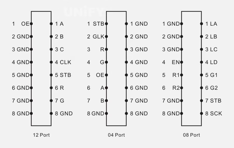
Figure 1-18: 08, 12, 04 Common Interfaces
ndoor LED displays often use the 08 interface, while outdoor LED displays mostly use the 12 interface, though it’s not the only one for outdoor use. When choosing a control card and unit board/module, try to ensure the interfaces are consistent. If not, the wiring can be modified based on the principles. LED display interface types are shown in Table 1-3.
Table 1-3 LED display interface types
Interface Type | 08Interface | 04Interface | 12Interface | ||||||||||||
Sort order | 1 3 5 7 9 11 13 15 | GND GND GND EN R1 R2 GND GND | LA LB LC LD G1 G2 STB SCK | 2 4 6 8 10 12 14 16 | 1- 3- 5- 9- 11- 13- 15- | STB CLK R G OE A B GND |
GND -2 GND GND -6 GND 8 GND 10 | 1- 3- 5- 7- 9- 11- 13- 15- | OE GND GND GND GND GND GND GND | A B C CLK STB R G- D | -2 -4 -6 -8 -10 -12 -14 -16 | ||||
Interface Type | 08Interface | 04Interface | 12Interface | |||
picture | ||||||
Commonly seen on 1/16 and 1/8 scans | Common in 1/4 sweep | Common in 1/4 sweep | ||||
HUB08 Interface pin definitions: Left 1: GND; 2: GND; 3: GND; 4: OE; 5: R1; 6: R2; 7: N; 8: GND Right 1: LA; 2: LB; 3: LC; 4: LD; 5: G1; 6: G2; 7: STB; 8: SCK
HUB12 Interface pin definitions: Left 1: OE; 2: GND; 3: GND; 4: GND; 5: GND; 6: GND; 7: GND; 8: GND Right 1: A; 2: B; 3: C; 4: CKL; 5: STB; 6: R; 7: N; 8: GND
LED displays have scanning methods such as 1/8, 1/4, 1/2, and static scanning. Their interfaces are all different. Common ones include HUB02, HUB08, HUB18, HUB75, and HUB40.
HUB02 Interface pin definitions (Indoor F3.75 full-color module): Left 1: A; 2: C; 3: CLK; 4: LAT; 5: R1; 6: G1; 7: B1; 8: D Right 1: B; 2: N; 3: N; 4: N; 5: R2; 6: G2; 7: B2; 8: OE
HUB18 Interface pin definitions (Indoor P7.62 full-color 1/8 module): Left 1: CLK; 2: LAT; 3: R1; 4: G1; 5: OE; 6: A; 7: B; 8: C Right 1: N; 2: N; 3: G2; 4: R2; 5: N; 6: N; 7: N; 8: D
HUB75 Interface pin definitions (Outdoor P10 full-color): Left 1: R1; 2: B1; 3: R2; 4: B2; 5: A; 6: C; 7: CLK; 8: OE Right 1: G1; 2: N; 3: G2; 4: N; 5: B; 6: N; 7: LAT; 8: N
HUB40 Interface pin definitions (Outdoor P16 full-color): Left 1: R1; 2: B1; 3: R2; 4: B2; 5: CLK; 6: ST; 7: OE; 8: N Right 1: G1; 2: N; 3: G2; 4: N; 5: N; 6: N; 7: N; 8: N
HUB39 Interface pin definitions (Outdoor P12 full-color 1/2): Left 1: S; 2: L; 3: R1; 4: G1; 5: OE; 6: A; 7: OE; 8: A; 9: B; 10: C; 11: S; 12: B1 Right 1: N; 2: N; 3: R2; 4: G2; 5: N; 6: N; 7: N; 8: N; 9: N; 10: N; 11: N; 12: B2
2. LED Unit Board Scanning Methods and Control Signals
(1) LED Unit Board Scanning Methods
Distinguishing LED Unit Board Scanning Methods. The simplest way to determine an LED unit board’s scanning method is to count the number of LEDs and 74HC595 chips on the board, then use a formula. For example, a unit board has 64×32 single-red LEDs and 16 74HC595s (one 6025 equals two 74HC595s). The calculation is: (Number of LEDs) / (Number of 74HC595s) / 8. So, 64×32 / 16 / 8 = a 16-scan. For another example: a unit board has 32×16 LEDs and 16 74HC595s. The calculation is: 32×16 / 16 / 8 = a 4-scan. Using the same LEDs, a 1/16 scan is brighter than a 1/8 scan. Indoor LED displays typically use a 1/16 scan, while semi-outdoor displays use 1/16, 1/8, or 1/4 scans. For displays in bright sunlight, a 1/4 scan is best.
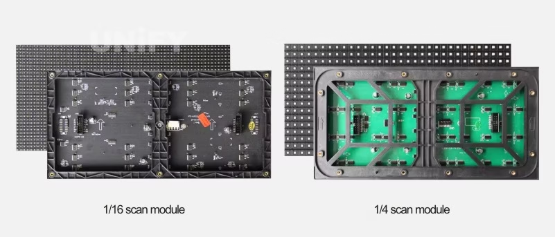
Figure 1-19: Unit Board Front and Back Views
The LED display row selection circuit is shown in Figure 1-20: Row Selection Circuit. Its purpose is to select and drive the corresponding rows. The 4953 chip in the diagram acts as an amplifier. In this circuit, the A, B, C, and D signals from the HC245 chip are connected directly to the 4953 chip without a 3-to-8 decoder. This circuit uses four signal lines (A, B, C, D) for row selection. When signal A is active, four rows are selected. Similarly, when B, C, or D is active, four rows are selected. A cycle is completed in four scans, hence it’s a 1/4 scan. Another way to understand the scanning method is that the circuit controls 16 rows using four signal lines, so 4/16 = 1/4, making it a 1/4 scan circuit.
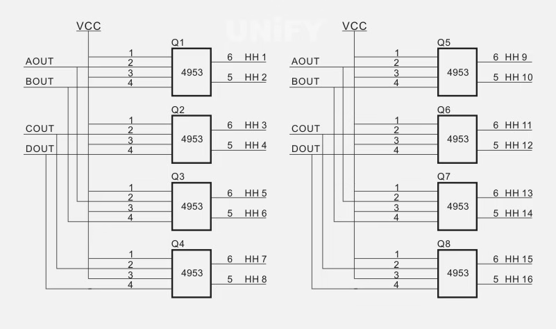
Figure 1-20: Row Selection Circuit
When determining the scanning method, besides looking at the A, B, C, and D signals, you must also check for a 3-to-8 decoder. If there are A, B, and C signals with one 3-to-8 decoder, it’s a 1/8 scan. If there are A, B, C, and D signals with two 3-to-8 decoders, it’s a 1/16 scan.
1/16 Scanning Wiring Method. To achieve a 1/16 scan, there are usually four signals: A, B, C, and D. You can use one 4-to-16 decoder or two 3-to-8 decoders to implement the 16-row scan. The 1/16 scanning wiring method is shown in Table 1-4.
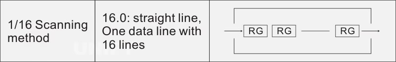
1/8 Scanning Wiring Method. Typically, the circuit board has three signals: A, B, and C. One 3-to-8 decoder can be used to implement an 1/8 scan. The 1/8 scanning wiring method is shown in Table 1-5.
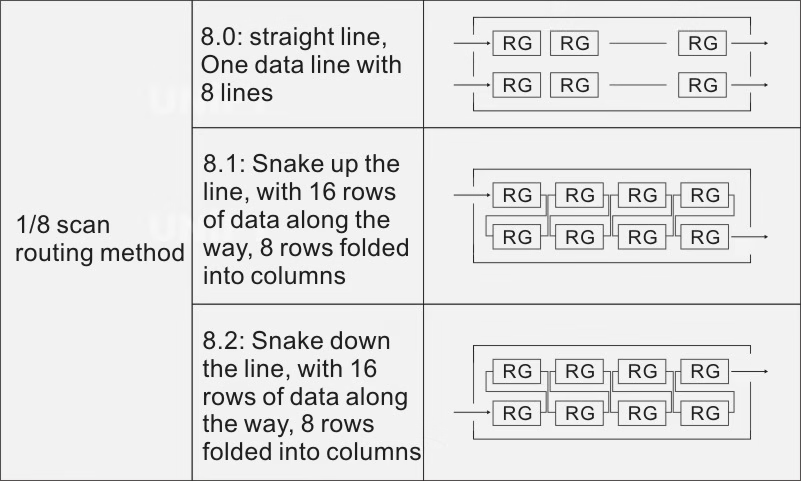
1/4 Scanning Wiring Method. Generally, the circuit board has two signals, A and B, and a 2-to-4 decoder can be used. If no decoder is used, four signals (A, B, C, D) are required, with each signal selecting one row. The 1/4 scanning wiring method is shown in Table 1-6.
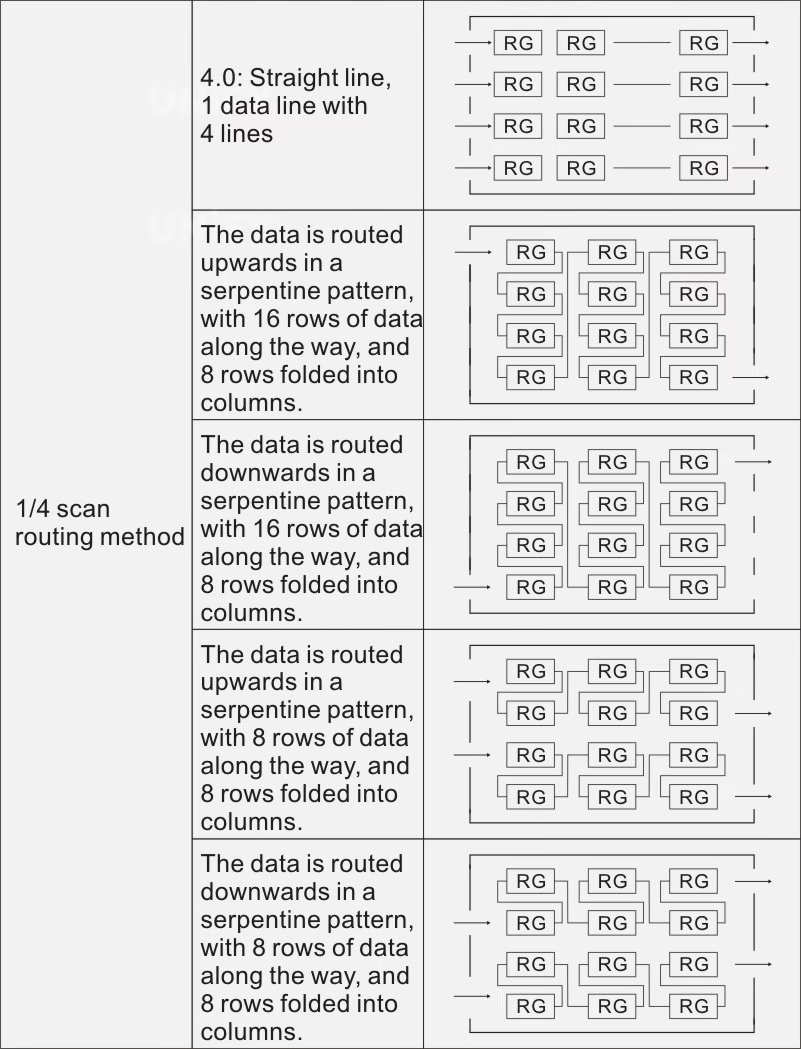
(2)LED Display Control Signals
LED Display Control Card. The LED display control card is the core component of the display. It receives display information from a computer’s serial port, stores it in frame memory, and generates the required serial display data and scan control timing based on a partitioned drive method. There are two types: synchronous LED control cards and asynchronous LED control cards.
Synchronous LED Control Card. This card is mainly used for real-time display of videos, graphics, and text. It’s primarily used for large indoor or outdoor full-color LED displays. Its operation is similar to a computer monitor, mapping images from the computer screen pixel-by-pixel in real-time at a refresh rate of at least 60 frames/s. It has multi-grayscale color display capabilities and can achieve rich multimedia effects. Its key features are: real-time performance, rich expressiveness, complex operation, and high cost. A typical synchronous control card setup includes a sending card, a receiving card, and a DVI graphics card.
Asynchronous LED Control Card. Also known as an offline card, it is used to display various texts, symbols, graphics, or animations. Display information is edited on a computer and pre-loaded into the display’s frame memory via an RS232/485 serial port. The content is then played screen by screen in a loop, offering a variety of display modes. Its main features are: simple operation, low cost, and a wide range of use. A simple asynchronous card can only display a digital clock, text, and special characters. A graphic asynchronous card, in addition to the functions of a simple system, can also control the content of the display by specific areas.
Control Signal Distribution. The back of an LED unit board is shown in Figure 1-21. Chip A (HC245) acts as a signal amplifier. Specifically, chip A1 (HC245) amplifies the signals for the top half of the board (the first and second sets of RGB data). Chip A2 (HC245) amplifies the signals for the bottom half (the third and fourth sets of RGB data). Chip A3 (HC245) amplifies the ABCD row signals, CLK, SC latch, and OE control signals. Chip A4 (HC245) amplifies all signals before they are sent to the unit board’s output interface. Chip B (TB62726) in Figure 1-21 is an LED driver chip, and its main function is to control the column display on the unit board. The B (TB62726) chips in columns 1 and 4 control the red LEDs, those in columns 2 and 5 control the green LEDs, and those in columns 3 and 6 control the blue LEDs. One TB62726 controls 16 columns, and a group consists of three TB62726 chips for red, green, and blue. Chip C (4953) in Figure 1-21 controls the row display. One 4953 controls two rows, so eight of them control 16 rows.
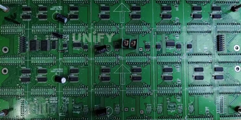
Figure 1-21: Back View of a Unit Board
Signal Path Analysis.
CLK, SC Latch, and OE Control Signals. The input signal first enters chip A3 (HC245) and chip A4 (HC245) simultaneously, then enters chip A2 (HC245) and chip A1 (HC245) simultaneously, and finally connects in parallel to each TB62726 chip.
ABCD Row Signals. The input signal simultaneously enters the red chips A3 (HC245) and A4 (HC245). The output from A3 (HC245) connects to four 4953 chips, and the output from A4 (HC245) also connects to four 4953 chips.
RGB Data Signals. The input for the first and second RGB data sets enters chip A1 (HC245), and the third and fourth sets enter chip A2 (HC245). The R1 data from the first set then serially enters chips B1 (TB62726) and B4 (TB62726); G1 data serially enters chips B2 (TB62726) and B5 (TB62726); and B1 data serially enters chips B3 (TB62726) and B6 (TB62726). The other RGB data sets follow the same pattern.
HUB Adapter Board Signal Distribution. The HUB adapter board is the final step in data transmission. It’s a card that splits signals from the control card into multiple branches. This is typically determined by the vertical number of modules on the LED display. Figure 1-22 shows a HUB adapter board. From Figure 1-22, you can clearly see the various signals. Signals travel from the HUB board via flat cables to the unit board or modules, completing data transmission. Besides data signals, which are transmitted serially, all other signals are transmitted in parallel.
CLK (Clock) Signal. This provides the shift pulse for the shift register. Each pulse causes data to shift in or out by one bit. Data on the data port must be synchronized with the clock signal to transmit correctly. The data signal frequency must be half of the clock signal frequency. If the clock signal is abnormal, the entire board will display garbled data.
STB (Latch) Signal. When a data transmission is complete, the STB latch signal becomes active, locking the data in the shift register and displaying it by lighting up the LEDs through the driver circuit. However, the driver circuit is controlled by the EN enable signal, so the enable signal must be active for the LEDs to light up. The latch signal must also be synchronized with the clock signal to display a complete image. If the latch signal is abnormal, the entire board will display garbled data.
EN (Enable) Signal. The EN enable signal controls the overall brightness of the LED display and is also used for blanking. By adjusting its duty cycle, you can control brightness. If the enable signal is abnormal, the entire screen may not light up, be dim, or show ghosting.
Color Data Signals. These signals provide the data needed for the image and must be synchronized with the clock signal to transmit data to each display point. Typically, in an LED display, the red, green, and blue data signals are separate. If a data signal is short-circuited to the positive or negative rail, the corresponding color will be fully bright or off. If the data signal is left floating, the color display will be unstable.
ABCD Row Signals. These only exist in dynamic scanning displays. ABCD are binary numbers, with A as the least significant bit. When using binary, the ABCD signal can control up to 16 rows (0000-1111). If the AB signals are used with the four states 00, 01, 10, and 11, they can control a maximum of 4 rows. This is decoded by the IC138D, which corresponds to one output, a four-to-one selection, also known as a 1/4 scan. If the row control signals are abnormal, the display may show misalignment, high brightness, or overlapping images.
Analysis of a monochrome P10 module’s operation: AB are the row scan data signals. A inputs to pin 2 of the IC245, is amplified and shaped, and outputs from pin 18. One path goes directly to the A pin on the output header; the other path goes to pin 1 of the IC138. B inputs to pin 3 of the IC245, is amplified and shaped, and outputs from pin 17. One path goes directly to the B pin on the output header, and the other path goes to pin 2 of the IC138. The IC138D is an 8-bit binary-to-decimal decoder. A P10 module only has A and B, so there are only four states (00, 01, 10, 11). The corresponding outputs are pins 15, 14, 13, and 12, a four-to-one selection, thus it’s a 1/4 scan. The IC138D is controlled by the OE enable signal.
OE is connected to pin 5 of the IC138 and is active low. It will only have an output when the OE signal is active. Therefore, controlling the duration (duty cycle) of the OE signal adjusts the display’s brightness. The OE signal goes from the input header to pin 4 of the IC245, outputs from pin 16, and is then inverted by the IC74HC04. As a result, it should be set to active high in the LED display control software. The IC4953 is the row start IC. Internally, it has two independent CMOS high-power transistors. Pins 1, 2, 7, and 8 form the first group; pins 3, 4, 5, and 6 form the second. Pins 1 and 3 are connected to the positive power supply. Pin 2 is the control signal input for the first group, and pin 4 is for the second. Pins 7 and 8 are the outputs for the first group (paralleled for high current and heat dissipation), and pins 5 and 6 are for the second. One IC4953 controls two rows, so four of them control eight rows. The first and fifth rows are started simultaneously with the same signal, as are the second and sixth, the third and seventh, and the fourth and eighth. T
his is a fold-over (or exchange) every four rows. The control system software must therefore use the corresponding start program. Additionally, the first and ninth, second and tenth, and eighth and sixteenth rows are connected. Each row is connected to a 100Ω resistor at the negative power supply for constant voltage. The CLK is the clock signal. It inputs from pins 5 and 6 of the IC245, splitting into CK1 and CK2. CK1 outputs from pin 15 of the IC245 directly to the CLK pin on the output header; CK2 outputs from pin 14 of the IC245 and connects to pin 11 of each IC595. STB is the latch signal. It inputs from pins 7 and 8 of the IC245, splitting into ST1 and ST2. ST1 outputs from pin 12 of the IC245 directly to the STB pin on the output header; ST2 outputs from pin 13 and connects to pin 12 of each IC595. R is the red column data signal. It inputs from pin 9 of the IC245. Pin 11 of the IC245 outputs to pin 14 of the first IC595 in the first row, then outputs from pin 9 of that IC. It then goes to pin 14 of the second IC595 in the first row, and the cycle continues. Finally, it outputs from pin 9 of the last IC595 to the output header pin.
Recommend Products
IPS Display vs LED Display: 2026 Ultimate Comparison Guide
Compare IPS display vs LED displays to find the perfect screen for gaming, professional design, or retail. Explore 2026 updates on color accuracy, brightness, and energy efficiency to maximize your ROI.

QLED vs Crystal UHD: Which Display Fits Your Business ROI?
Compare QLED vs Crystal UHD for commercial displays. Learn which technology fits your budget, limits of LCD, and when to upgrade to seamless LED Video Walls.
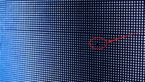
How to Repair P6 Outdoor LED Display Sign Board Screen
Learning how to repair P6 outdoor LED display sign board screens requires expert knowledge. Discover our step-by-step guide on module replacement, waterproof sealing, and color calibration.